


[067] Flyback Development Part IV- Current Sense, Snubbing, Regulation
Flyback design transformer and full power testing.
Introduction
This article is the fourth of a series in which Dr. Ridley shows the steps involved in designing and building an offline flyback converter. The power transformer is added to the circuit, and the current sensing and snubbers are designed to operate at full power without excessive stress on the components.
Power Transformer Testing

Figure 1: Schematic of the flyback converter. After the transformer is inserted, the elements in green have to be selected and tuned.
Figure 1 shows the schematic of the flyback converter with the transformer inserted into the circuit. Before applying the full load on the circuit, the elements in green have to be selected and tuned for proper operation.
Current limiting is key to reliable operation of PWM converters. At low power levels, a sense resistor in series with the power FET is adequate to detect the current flowing when the switch is on. Design of this resistor is such that the peak voltage is just below the maximum allowed voltage at the input to the PWM comparator. For the 384x series of controllers, this is limited to 0.9 V, and most PWM controllers have a similar limit. For offline design, this voltage drop across the sense resistor does not represent significant power loss. With higher power converters, the use of a current transformer is recommended.
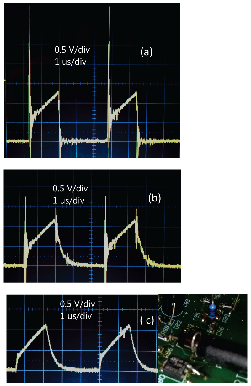
Figure 2: Primary current-sense signals (a) at source of FET (b) after RC filter and (c) with proper probe placement.
Figure 2a shows the raw unfiltered waveform on the source of the FET. There is a large leading-edge spike due to parasitic resistances and reverse recovery of the secondary diode, and this has to be filtered with an RC network so that it does not trip the PWM comparator.
Figure 2b shows the waveform after the filter. It is still very noisy, but this is due to the probing technique used. If the tip of the scope probe and the ground lead is removed, and the scope probe connected very close to the test points, the waveform of Figure 2c results. Now it can be seen that there is a clean signal. The leading edge spike is removed, but the waveform is not so heavily filtered that the current sense information is lost.
The proper test for correct filtering is that there should be no false triggering, but also no current runaway on startup of the converter. This should be tested early on in the design process (after the snubber design below) to make sure that the circuit is properly protected.
Primary Clamp Design
Figure 3 shows the primary switch drain waveform for the main power FET. The clamp circuit was designed using a high-speed, fast recovery diode and a 0.01 µF capacitor. The resistor was selected by the design program POWER 4-5-6, but was subsequently adjusted in value by circuit observation. The lower the value of resistor, the harder the voltage on the FET is clamped, but at the expense of higher power dissipation. You can find an article analyzing this process in reference [2].
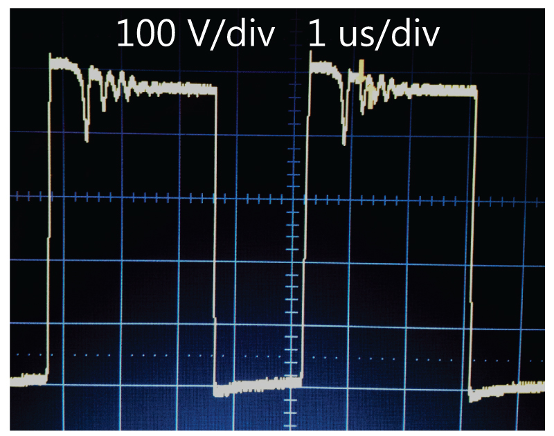
Figure 3: Primary switch drain waveform with RCD clamp.
Secondary Snubber Design
After designing the primary clamp, the secondary snubber was addressed. During the process of looking at the secondary diode voltage, the ground of the scope probe inadvertently touched the wrong node of the circuit, resulting in an explosive failure. (Normally when writing papers, researchers don’t mention the failures. However, for those of you who are new to power supply design, this is a standard part of the process. You will make mistakes, and with high-voltage power supplies, they will result in catastrophe sometimes.)
In this case, the components in red shown in the circuit diagram were destroyed, including the FET, control chip, gate resistor, current sense resistor, and current filtering resistor. Even seasoned power supply designers have failures in their circuits [3], and this is often exacerbated by the dense packaging of modern electronics.
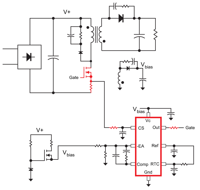
Figure 4: Components in red failed after touching the wrong circuit node with the voltage probe, shorting the transformer secondary.
With the failed circuit components replaced, the waveforms shown in Figure 5 were observed on the main output diode. There was very substantial ringing due to the hard reverse recovery of the diode, and an RC snubber needs to be added to damp this. This is done according to the process to be found in reference [4].
Even after the RC snubber was added, there is significant overshoot on the diode. This can be fixed as in the primary by using an RCD clamp. Normally this is not done on the secondary side of a flyback, but it is an option if you want to use a lower voltage part for better efficiency. Of course, the dissipation in the RCD clamp will impact the efficiency, too.
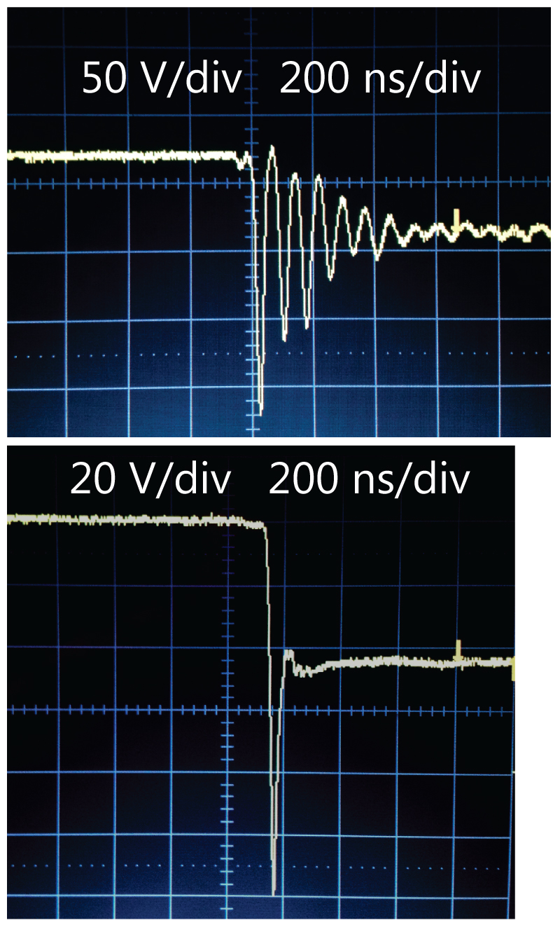
Figure 5: Secondary diode waveform before and after RC snubber is added. The peak stress from the voltage spike can be reduced if an RCD clamp is used on the secondary side.
The reverse spike can also be eliminated by choosing a much smaller magnetizing inductance of the power transformer, and running the converter in DCM. In this case, higher currents will flow in the switch as a tradeoff to the elimination of the spike. The optimal design point for your power converter will depend on many factors, and trying different transformers and values experimentally is a useful process.
Full Power Operation and Regulation
It is convenient early in the testing process to close a loop on the converter, even though you may not be ready to do full control analysis and an aggressive design. For low power circuits, you can add a large capacitor C3 in the circuit from the –EA to the COMP pin, in this case 4.7 µF was used. The value of the resistor R1 in Figure 1 was chosen to be 100k, and Rb was chosen to set the feedback voltage to be 15 V.
The combination of R1 and C3 form a low-gain integrator, and this allows the circuit to regulate on a slow basis. This is convenient for doing experiments on the power stage and transformer, and for verifying the DC regulation of a converter early in the design process.
(This is not necessarily a recommended procedure for high power converters. The very slow loop created allows for a large voltage overshoot on the output during startup and transient events, and this can potentially cause damage to the converter or to the loads.)
| Main Output Voltage | Output Current |
| 15.03 V | 0.43 A |
| 14.59 V | 1.02 A |
| 14.26 V | 1.55 A |
| Regulated Bias Output 15.02 V | 30 mA |
| Main Regulation Band | 5.2% |
Table 1: Output voltage regulation data with different loads.
For this flyback converter design, as for the forward converter in reference [5], the objective was to regulate from the bias winding, and to design the transformer in such a way that the main output tracked the auxiliary output as closely as possible. With good tracking, an optocoupler and feedback amplifier (typically a TL431) can be avoided in the circuit design, saving parts cost and complication. As you can see from the Table 1 above, the total voltage range was 5.2% with a 4:1 load range on the main output. Since the output voltage here was designed to be used to feed another switching regulator, the much variation is acceptable.
The regulation can be improved with more loading on the bias output, but this has a big impact on light load efficiency. In some modern green power applications, the additional dissipation is not acceptable.
Summary
The fourth part of this series has described the current sensing, clamp and snubber design for the flyback converter.
References
- Power 4-5-6 design software
- Flyback Converter Snubber Design Article [11]
- LinkedIn Power Supply Design Center group. See discussion on “Power Supply Failures”
- Snubber Design Article [A39]
- Power Supply Development Diary, Parts I – XV11