


Using the switch model to analyze the tapped boost converter.
Introduction
This article reviews shows how the simple and elegant PWM switch model, developed by Vorpérian in 1986, can be identified in more complex circuits such as the tapped boost converter. Straightforward rearrangement of the circuit reveals the PWM switch structure.
PWM Switch Modeling
As mentioned in the last article of this series [1], Dr. Vatché Vorpérian developed the PWM switch model in 1986, which replaced the need for state-space averaging and greatly simplified the analysis process. It was a very elegant and intuitive modeling approach, which is easily grasped by new students in the field.
Figure 1 shows the PWM switch arrangement identified by Dr. Vorpérian in gold. Once this configuration of switch and diode is found in the power circuit, it can be replaced by one of three equivalent circuits, depending on what kind of analysis is to be done.

Figure 1: PWM switches and the three equivalent circuits used for different types of analysis
The equivalent circuit outlined in red is the nonlinear PWM switch model. This can be used in Spice to find both DC and AC analysis, if desired. The nonlinear model can also be used to generate distortion characteristics of switched-mode amplifiers and other circuits that operate over a large range of conditions. However, its nonlinear nature makes it unsuitable for hand analysis if you are trying to arrive at symbolic result for complete circuit understanding.
Tapped Boost Converter
To perform the PWM converter circuit analysis, it is crucial to find the switch and diode circuit structure shown in Figure 1. However, in some PWM circuits, it doesn't exist in the original circuit diagram. In the previous article, we showed how it could be found in isolated topologies, a straightforward process. In [2], it was shown how it can be found for the Sepic converter.
Figure 2 shows another interesting topology, the tapped boost converter. The power FET is connected to a middle winding of the inductor as shown, and the diode is connected to the end of the winding. This circuit is useful if a large step-up ratio is required from the circuit operation.
When the FET is on, the inductor has less than the complete number of turns connected, and the current shown in red results. When the FET turns off, the inductor now has the complete number of turns in series with the diode. The current is reduced by 1/(1+n) relative to the FET current, and the diode waveform is shown in green.
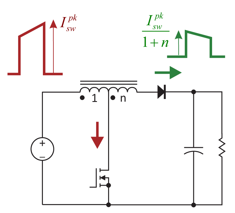
Figure 2: The tapped boost topology. This circuit can be useful for large step-up ratios, but the connection of the switch and diode is not present in the original circuit.
Figure 3 shows the sequence of circuit manipulations needed to find the PWM switch model. In the top circuit, no connections are changed, but the inductor is redrawn as a transformer with a 1:n ratio. This is not an ideal transformer, but it has a finite value of magnetizing inductance which defines the energy storage inductor value. (This is similar to component always drawn for a flyback converter: the transformer is shown explicitly, but value of the magnetizing inductance is a critical design element.)
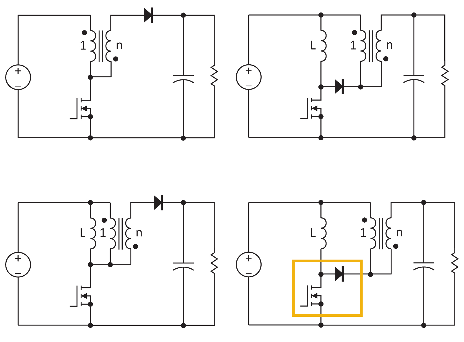
Figure 3: Rearrangement of the tapped boost circuit reveals the PWM switch structure, allowing analysis to be done using Vorpérian's switch model.
The inductor itself is explicitly shown in parallel with the transformer in the second circuit, and the value is that seen with just the left hand turns count. The 1:n transformer is now ideal with an infinite value of magnetizing inductance.
With an ideal transformer, the diode connected on the secondary side can now be moved to the primary. The direction is important to define proper operation of the circuit. In the original circuit, the diode only allows current to flow into the dot of the secondary winding. When the diode is moved to the primary, it can only allow current to flow out of the dot as shown in the third circuit of Figure 3.
The PWM switch arrangement is now obvious, and it is framed in gold in the fourth circuit of Figure 3.
DC Analysis of the Tapped Boost Converter
Now that the switch model has been identified, it is a simple matter to proceed with analysis of the circuit. Figure 4 shows the DC switch model in green substituted for the switch-diode combination, and we use this equivalent circuit to find the DC conversion ratio of the tapped boost circuit.
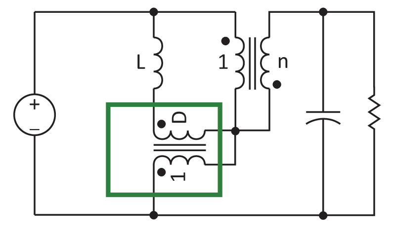
Fig. 4: In order to solve for the DC gain of the circuit, the DC switch model is substituted for the original switching elements.
Notice that the 1:D transformer of the DC model is not connected in a way that allows simple inspection for the circuit to find the gain. Solving the DC gain of the circuit is an exercise in applying Kirchoff's voltage law. Two voltage loops are identified for the circuit as shown in Figure 5.
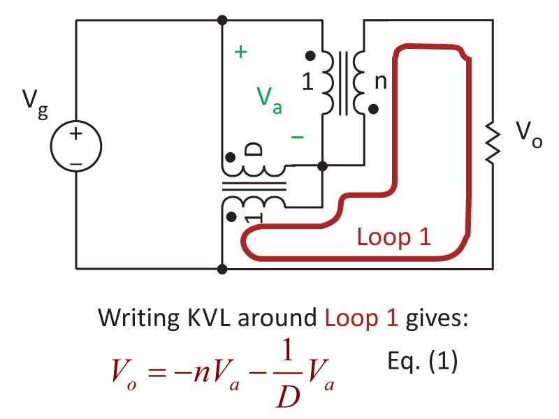
Fig. 5: Solving for DC gain by applying KVL around the first loop of the tapped boost circuit.
First, we assign a value of Va to the voltage across the two circuit transformers as shown in green. Then, moving around the loop in red, Equation (1) in Figure 5 gives the relationship between the output voltage and Va.
The second loop is shown in Figure 6, and this allows us to solve for Va in terms of the input voltage, Vg. Substitution of this equation into the first equation gives the gain of the tapped boost circuit, as outlined by Equation [3] in green.
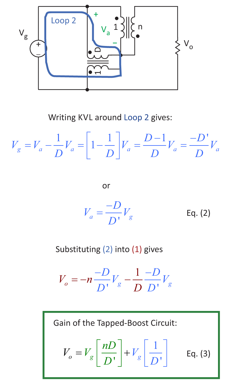
Fig. 6: Solving for DC gain by applying KVL around the second loop of the tapped boost circuit.
Notice that there are two terms making up the gain of the tapped boost converter. The second term, shown in blue in Equation [3], is the same as the gain of a normal boost converter. The first term, shown in green, is the same as the gain of a flyback converter, but without any inversion. If the secondary turns ratio is zero, we have just a normal boost converter, as would be expected.
With a turns ratio of one, at a 50% duty cycle, the gain of the circuit is 3, instead of the usual gain of 2 that would be obtained with just a boost converter. This demonstrates the advantage of this topology, giving increased gain. However, it does not come for free, and it has all the problems of transformer-isolated circuits. Most notably the effect of leakage inductance between the two windings causes voltage spikes on the power FET.
Summary
This article has described how to find the PWM switch model in the tapped boost circuit. This lets us find the DC gain of the circuit with ease, as has been shown. The ac analysis is also straightforward if we substitute the ac circuit model.
Tapped inductor circuits are often suggested as solutions to interesting power conversion problems. The tapped buck is useful if we want to arrive at large step-down ratios. For all of these types of converters, it is usually just a straightforward manipulation of the circuit to find the switch model. Not many designers practice this kind of circuit analysis these days, but it is a useful skill to have.
The PWM switch model was discussed in great detail when it was first discovered at conferences and in industry papers, but is now assumed to be background knowledge. I often find that many of our workshop attendees [3] are not aware of the existence of these modeling tools, and it is important to introduce them to the simplicity of PWM switch model application to their circuits.
References
- PWM Switch Model Review, Article [69],
http://www.ridleyengineering.com/design-center.html - Analyzing the Sepic Converter, Article [02],
http://www.ridleyengineering.com/design-center.html - Power Supply Laboratory Workshop,
http://www.ridleyengineering.com/workshops.html - To learn how to make control measurements, please visit
http://www.ridleyengineering.com/analyzer.html - Join our LinkedIn group titled “Power Supply Design Center”.Noncommercial site with over 7000 helpful members with lots of experience.