


Design equations and analysis of the most commonly-used RCD clamp circuit used for the popular flyback converter.
Introduction
All PWM converters have parasitic components that lead to ringing waveforms which must be properly suppressed. Without this, semiconductors can fail, and noise levels will be higher than necessary. This article describes the most commonly-used RCD clamp circuit used for the popular flyback converter, together with its design equations.
Flyback Converter with No Snubbers
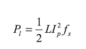
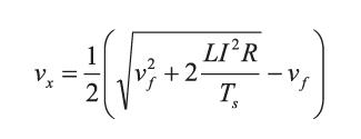
Without a snubber, the leakage inductance of the flyback transformer rings with stray capacitances in the circuit, producing large amplitude high-frequency waveforms as shown in Figure 1.
Many application notes and designs ignore the ringing waveforms and operate the converter without addressing the issue. There are two problems with this: firstly, there is excessive voltage on the drain of the FET which can lead to avalanche breakdown and eventually failure of the device. Secondly, the ringing waveform will be radiated and conducted throughout the power supply, load, and electronic system, creating noise issues and even logic errors. The ringing frequency will also show up as a peak of the EMI spectrum in both radiated and conducted EMI.

Figure 1: Flyback converter drain voltage
In most designs, this is not acceptable, and it is necessary to add circuit elements to damp the ringing (using an RC snubber), or to clamp voltages (with RCD clamps), or both. The design of these networks is a combination of measurements and analysis to ensure a rugged and dependable result.
Primary RCD Clamp for the Flyback Converter
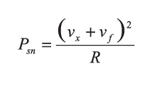
Figure 2 shows an RCD clamp circuit used to limit the peak voltage on the drain of the FET when an RC snubber is insufficient to prevent switch overvoltage. The RCD clamp works by absorbing the current in the leakage inductor once the drain voltage exceeds the clamp capacitor voltage. The use of a relatively large capacitor keeps the voltage constant over a switching cycle.
The resistor of the RCD clamp always dissipates power. Even with very little load on the converter, the capacitor will always be charged up to the voltage reflected from the secondary of the converter, vf. As the load is increased, more energy will flow into the capacitor, and the voltage will rise by an additional amount, vx, above the ideal square wave flyback voltage. The waveform defining these voltages is shown in Figure 2.
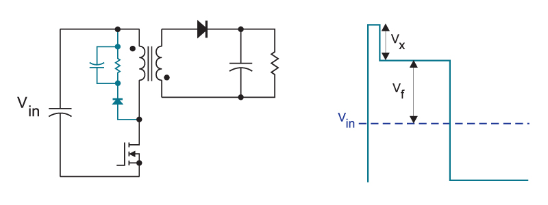
Figure 2: Flyback converter with primary RCD clamp
Design Step 1 – Measure Leakage Inductance
It is important to measure the leakage inductance of the flyback transformer prior to designing the snubber. Details of how to do this are given in [1]. Do not just guess at the value of inductance, and be aware that worst-case specifications from magnetics manufacturers are often not accurate enough to use for design. Also, as explained in [2], the leakage inductance is a frequency-dependent, and must be measured at the proper value of frequency.
Design Step 2 – Determine Peak Clamp Voltage
Now you must decide how much voltage can be tolerated on the power MOSFET, and calculate the amount of power that will be dissipated in the clamp with this clamp level. The power associated with in the leakage inductance, L, with a current worst-case current Ip at turn-off is given by:
Analysis of the RCD snubber has appeared in papers and numerous application notes. It is assumed that there are no stray capacitances to charge, and that all the leakage energy is conducted into the snubber capacitor from the leakage inductance. The capacitor is assumed to be large enough that its value does not change significantly during one switching cycle.
With these assumptions, the power dissipated by the RCD clamp can be expressed in terms of the energy stored in the inductor as follows:
In other words, the higher we let the clamp voltage rise on the switch, the lower the overall dissipation. But of course, we must balance this against the total voltage seen across the power FET, so we cannot arbitrarily reduce dissipation.
A typical design is for the voltage vx to be equal to ½ the flyback voltage. In this case, the dissipation is equal to 3 times the stored energy in the leakage inductance, which is not an immediately intuitive result. This is a conservative estimate, however. It does not account for lossy discharge of the inductor, nor for stray capacitance. In reality, the design will have less loss in the clamp than anticipated due to these effects.
For high-voltage offline designs which are often constrained to use a FET with a maximum voltage of 650 or 700 V, the voltage vx will have a hard limit set by the maximum input line, maximum current, and FET breakdown voltage. Do not exceed the stated Vds of the FET, and be aware that the breakdown can vary with temperature. Some designers rely on the avalanche capability of the FET to let them regularly exceed the breakdown voltage. This is not recommended for rugged power supply design.
Design Step 3 – Select Clamp Resistor
The capacitor of the snubber needs to be large enough to keep a relatively constant voltage while absorbing the leakage energy. Apart from this consideration, its value is not critical, and will not affect the peak voltage when the snubber is working properly.
The resistor is the element that is crucial in determining the peak voltage vx, and it should be selected with the following equation:
A larger value of resistor will slow the discharge of the clamp capacitor, and allow the voltage to rise to a higher value. A smaller value will result in a lower clamp voltage, but the dissipation will be increased.
Design Step 4 – Calculate Power Loss
The snubber design is now complete, but we often need to know what the dissipation will be for currents other than the worst case current, Ip, in the equations above. Use the following equation to calculate the voltage rise in a known snubber for a given peak current I, and leakage inductance L.
The value of the voltage rise, vx, above the flyback voltage is given by:
The power dissipation is given by:
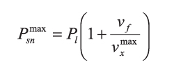
Design Step 5 – Experimental Verification
Experimental verification of the design is essential since there will be effects not accounted for in the equations, and your circuit will have nonideal components. Figure 3 shows the effectiveness of the circuit in clamping the peak value of the FET drain voltage.
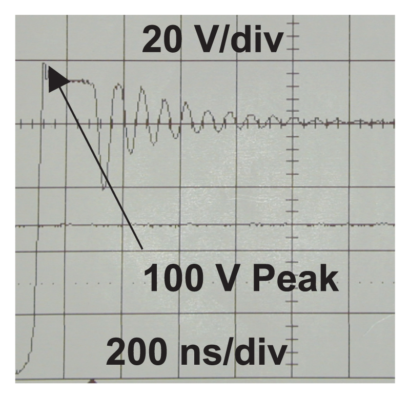
Figure 3: Flyback converter drain voltage with primary RCD clamp.
This figure also shows a limitation of the RCD clamp. After the clamping period is finished, the circuit resumes ringing. With ideal components, this would not happen. However, the diode of the RCD clamp has a finite reverse recovery time which allows the leakage inductor current to flow in the opposite direction in the diode, resulting in ringing. The type of diode chosen for the RCD snubber is crucial. It must be as fast as possible with the proper voltage rating.
The severity of this ringing will depend on the reverse applied voltage across the RCD diode. The higher you allow the clamp voltage to climb, the lower the dissipation, but higher voltage and dv/dt is applied to the diode, and the ringing increases.
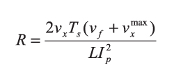
The ringing can subsequently be damped out again by introducing the RC snubber, designed as described in [1]. Figure 4 shows the drain waveform with both an RCD clamp and RC snubber in place. This provides the best protection for the FET, and the lowest EMI signature, but results in the highest power dissipation.
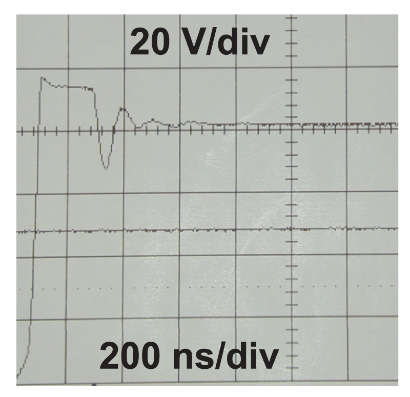
Figure 4: Flyback converter drain voltage with primary RCD clamp and RC snubber
Summary
The RCD clamp circuit is useful for all flyback converters to reduce the stress on the power FET. Make sure that the clamp is designed to restrict the voltage under worst-case operating conditions (high line, and maximum current limit) to less than the voltage rating of the part. The design equations in this article remove the guesswork from the clamp design.
Additional Reading
- Join our LinkedIn group titled “Power Supply Design Center”. Noncommercial site with over 7000 helpful members with lots of theoretical and practical experience.
- For power supply hands-on training, please sign up for our workshops.
- “Flyback Converter Snubber Design”