[071] Designing Snubbers for Nonisolated Converters
How to design snubbers when you don't know the inductance causing the ringing.
Introduction
This article shows how to design a snubber for circuits where the ringing inductance is not a defined quantity. This applies to nonisolated converters where PCB layout and component leads are responsible for the bulk of the inductance.
High-Frequency Switching Cell
All power electronics circuits with devices which rapidly turn on and turn off will exhibit voltage ringing when currents are interrupted or initiated. For transformer-isolated designs, the leakage inductance of the transformer usually dominates the ringing inductance, and the first step in snubber design is to measure this inductance value. This process is described in detail in references [1] and [2].
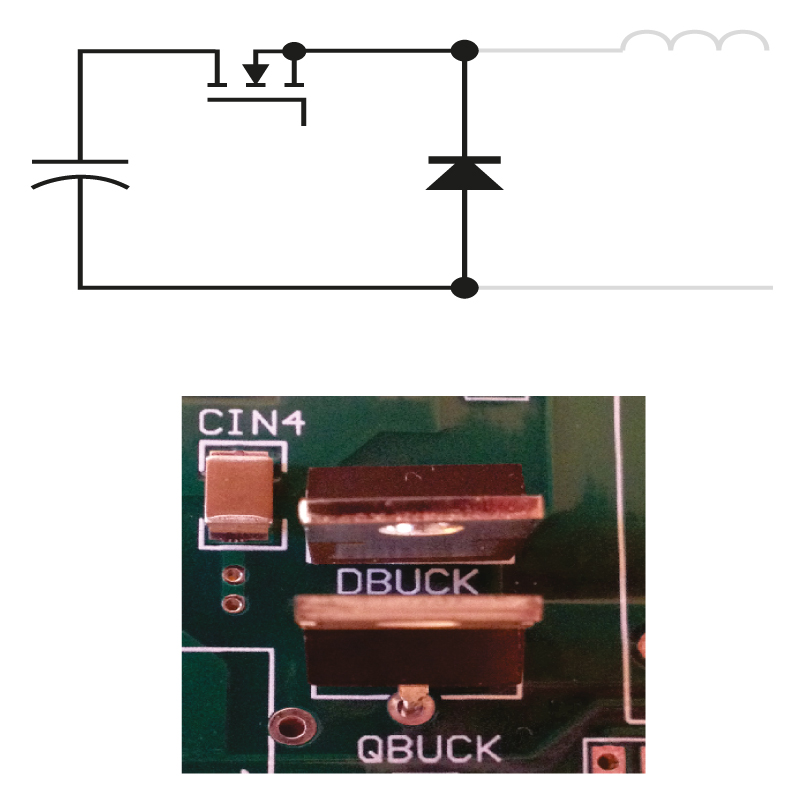
Figure 1: Buck Switching Cell and Circuit Placement
For a buck converter, there is no transformer, and no clearly-defined value of inductance with which to begin snubber circuit design. Figure 1 shows the schematic of the input side of a buck converter with the FET, diode, and bypass capacitor forming the high-frequency current loop. The PCB layout of this part of the circuit is also shown in Figure 1. As discussed in [3], the PCB layout should keep any high frequency current loops as small as possible in order to minimize the stray inductance. Even when this has been done, at higher power levels and with large discrete devices, it is inevitable that some stray inductance will remain in the circuit. Ringing will be a problem that has to be properly controlled in order to avoid excessive noise and stress.
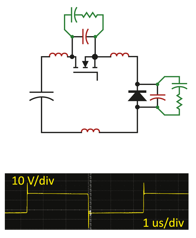
Figure 2: Stray Inductance Associated With Board Traces and Component Leads Rings With Diode Output Capacitance When It Turns Off
Figure 2 shows the inductance elements on the schematic. (Of course, on your production schematic, these elements don’t actually appear, but they will still cause trouble.) This inductance is formed by the board traces, component leads, and internal component wiring of the die-attachments. The output capacitance of the diode will ring with the inductance of the circuit.
Unfortunately, neither the L or the C that form the ringing are simple to define. The diode capacitance is a nonlinear value which changes with applied voltage. We also have to account for package capacitance to heatsinks in some cases. Measuring the L and C directly is difficult due to the small and variable values.
Ringing Waveforms
While the loop shown in Figure 1 on the PCB is small, it creates enough inductance to produce considerable ringing as shown in the oscilloscope waveforms of Figure 3.
Figure 3: Ringing on FET Turn-On
The top waveform of Figure 3 shows both the turn-on and turn-off ringing. The ringing on the leading edge occurs when the switch turns on, and the diode turns off. The expanded waveform of Figure 3 shows that this ringing frequency is approximately 47 MHz.
In order to damp the ringing frequency effectively without iteration, it is important to know one of the resonant values, either the L or the C. Without a transformer, L is a difficult measurement, so we will focus on finding the equivalent capacitance.
Determining Capacitance Value
You can look at datasheets to get an estimate of the capacitor value, and you will see the varying values with voltage. There are also variations in fabrication that lead to typical and maximum values, but no minimum value.
I always like to do an experimental verification of the diode capacitance. The procedure for this is as follows:
- Measure the ringing frequency.
- Add a known capacitance across the diode
- Measure the new ringing frequency.
- Repeat until the new frequency = 0.707 times old frequency. The added capacitor is then equal to the intrinsic capacitance.
It is very important when you do this that the added capacitor does not have long leads attached. These will substantially change the inductance of the circuit, and that will also lower the ringing frequency.
Adding a Parallel Discrete Capacitor Provides Estimation of Circuit Capacitance.
Figure 4 shows the ringing frequency of the turn-off of the diode with a 470 pF ceramic capacitor added in parallel with the diode. The ringing frequency is reduced to about 33 MHz. This corresponds to the required reduction of the frequency, indicating that 470 pF is the equivalent average value of the diode capacitance.
With this value of capacitance, and a 47 MHz ringing, the stray inductance of the circuit is calculated to be about 24 nH.
Snubber Resistor Value
The snubber design is completed by selecting the resistor needed, and calculating its power dissipation. I always start the design of the snubber with the resistance equal to the impedance of the capacitor at the ringing frequency, in this case about 7 ohms.
Fig. 5: RC Snubber Eliminates Ringing, But Overshoot Is Still Present
The dissipation in the resistor is approximately equal to the energy stored in the capacitor multiplied by the switching frequency, or about 0.05 W in this case.
The entire design process is repeated for the second switching incident when the FET is turned off. A different resonant frequency will be observed since the FET capacitance will be different to the diode capacitance.
Figure 6 shows the resulting waveform with both the FET and diode snubbers in place in the circuit. Leading and trailing edge spikes can be observed, but the sustained ringing is suppressed quickly.
Fig. 6: The Design Process Is Repeated For The FET Snubber.
Summary
Snubbers are crucial to include even in non-isolated converters. With very tight layout, the inductance can be minimized and this will reduce the peak overshoot on the ringing voltage.
This article has described how to design snubbers from empirical measurements when the ringing inductor value is unknown. A series of short experiments allows the design of the snubber in a single attempt, and the dissipation in the snubber is kept to a minimum.
References
- Join our LinkedIn group titled “Power Supply Design Center”. Noncommercial site with over 7000 helpful members with lots of theoretical and practical experience.
- For power supply hands-on training, please sign up for our workshops.
- Flyback Circuit Snubber Design, Article [A39],
http://www.ridleyengineering.com/design-center.html - Transformer Impedance Measurements, Article [46],
http://www.ridleyengineering.com/design-center.html - Power Supply Development Diary Part XI, Article [44],
http://www.ridleyengineering.com/design-center.html


