


Point-of-load converter loops need to measured as they push the state-of-the-art in crossover frequencies.
Introduction
Recent changes in component technologies have led to point-of-load power converters that are pushing the boundaries of control-loop performance. The need to break open and measure the loop is more essential now than ever before if lifetime system stability is to be guaranteed.
High-Frequency Point-of-Load Buck Converters
There has always been a debate about how essential it is to measure the loop of a switching power supply. Some power designers have always resisted this part of development and design validation, claiming they are able to tune a loop properly through step-load testing [1]. While this may have worked with low performance power supplies, it is increasingly difficult with modern high-performance systems
Seven things have happened in recent years that have brought the loop testing issue back to the forefront. These issues combine to create a much higher risk of power supply instability.
- Power converter switching frequencies have been raised significantly to 2 MHz or more.
- Multiple point-of-load power supplies are incorporated on a single electronics assembly
- Input and output capacitors are comprised of just multilayer ceramics with negligible ESR
- Each converter minimizes the output capacitance to reduce board area
- Loop gains have become very aggressive in order to meet step-load requirements
- Some or all of the power supply compensation is internal to the integrated power supply
- Voltage-mode control is being used in place of current-mode control
Most application notes for these supplies tend to imply that their design is straightforward, and no more complicated than putting a linear regulator on the board. This can get many system designers into trouble. Now let’s look at each of these seven risk issues.
1. High Switching Frequencies
Switching frequencies have risen substantially in the last 10 years as more and more regulators are forced onto boards in close proximity to the processors that they are supplying. 100 kHz switching is no longer sufficient since it results in large inductors and capacitors that simply won’t fit in the space available.
As switching frequencies climb, much greater demands are placed upon feedback amplifiers and layout. Both the power stage and feedback networks can exhibit small-signal and large-signal behaviors that are not accurately predicted by the modeling.
2. Multiple Converters on Assembly
With so many regulators on a board, the probability of a marginal design increases. Furthermore, proper testing of each regulator can seem daunting and overly time-consuming. If the makers of the parts do not suggest loop gain testing, it is unlikely than non-power engineers will even consider doing any. And when the power supplies are designed into the boards, there are usually no provisions made for loop. This can either increase the difficulty of test, or sometimes render it impossible when traces are placed in inner layers that are not accessible.
3. Multilayer Ceramic Capacitors
Multilayer ceramic capacitors have extremely low esr values, and very little capacitance is needed to meet output ripple requirements. Hence the power supply makers can minimize the design area, leaving it up to the electronics assembly designer to add more capacitance as needed. On the input side of the converter, if additional filtering is used for noise attenuation, a series inductor can resonate with the low-esr capacitors to form a peak in filter output impedance. This can lead to classic input filter oscillation issues [2].
4. Minimum Output Capacitance
As the output capacitance reduces, the converter is far more sensitive to capacitive loading. In the earlier days of power supply design, the capacitance in the converter would dominate any loading capacitance, making the loop response relatively impervious to any additions. This is no longer true, and local bypass capacitance at the load can be significantly larger than the power supply capacitance for which the loop has been optimized.
5. Aggressive Loop Gains
Most power supplies in the past would have loop gains which were very conservative. It is not unusual to find a crossover frequency of just 1 kHz or less for a 100 kHz converter. This is rapidly changing for point-of-load converters. It is not uncommon now to find loop gains well in excess of 1/10 the switching frequency. As this crossover frequency increases, the power stage models become less reliable, and the measured response does not follow theory so closely. Also, with high crossover frequencies, the gain-bandwidth of the error amplifier becomes a limiting factor.
It is essential to verify these more aggressive loops if long-term instability is to be avoided.
6. Internal Compensation
Many of the new low-power switching regulators remove the burden of compensation from the user, and they include the compensation components inside the IC. This can either be just the feedback compensation components R2, C1 and C3 shown in Figure 1, or it can include the input compensation components R1, Rb, C2 and R3 as well.
The problem with this integrated approach is that the compensation components are optimized for an assumed value of L and C in the power stage. If these values change, as is almost always the case, there is no opportunity for the user to properly compensate the power stage to achieve the best loop design.
7. Voltage-Mode Control
The great benefits of current-mode control are adaptivity to the inductor value, elimination of the LC filter resonance, and naturally optimal control in either CCM or DCM regions of operation. The main downside of current-mode has always been difficulty of implementation due to worsened signal-to-noise ratios in the modulator. This last problem is exacerbated as frequencies climb, so many integrated power supply makers have reverted back to voltage-mode control. This brings back in all of the lack of adaptivity of the loop design, and the loop gain and phase margin are much more susceptible to component variation.
In the rest of this article, we will look at how the output capacitor size interacts with loop bandwidth and the output step-load response
Effect of Capacitance on Step-Load Response
Figure 1 shows the schematic of a buck converter with a synchronous rectifier and MLC output capacitor.
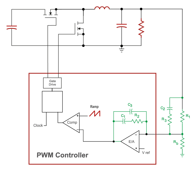
Figure 1: 400 kHz Buck Converter with Synchronous Rectifier and MLC Output Capacitor. Output voltage is 1.2 V at 20 A. Input Voltage is 12 V.
At a 400 kHz switching frequency, the impedance of the output capacitor is very small and easily able to attenuate the ripple current seen from the inductor. With MLC capacitors, the value of capacitance is chosen according to the step load requirements of the system rather than the ripple requirements. During the loop response time, the output capacitor has to absorb the energy stored in the output inductor when the load is turned off, and it must hold the output voltage within the regulation band when the full load is reapplied.
Figure 2 shows the overshoot on the output voltage when the load is decreased from 20 A to 4 A. The peak overshoot is 200 mV with a capacitance of 330 µF and a loop crossover frequency of 40 kHz.
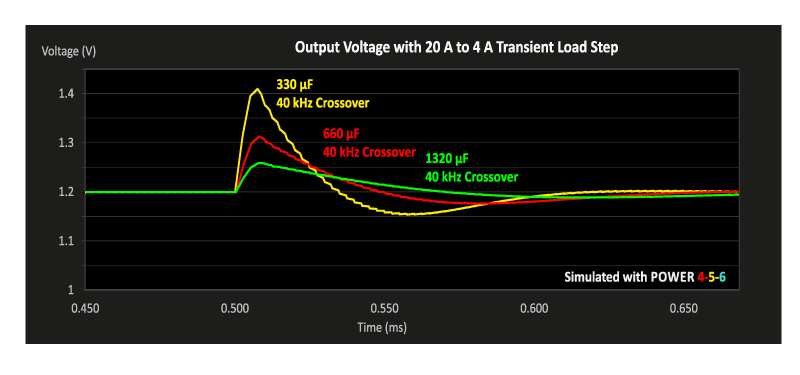
Figure 2: Output Voltage Response for Load Step From 20 A to 4 A with Different Capacitor Values
The overshoot can obviously be reduced if the output capacitance is increased. However, the benefits of the larger output capacitor are only fully realized if the loop gain crossover frequency can be maintained at 40 kHz. This requires different compensation each time the capacitor is changed.
Effect of Loop Gain Crossover on Step-Load Response
Figure 3 shows the step-load response of the same converter with a 330 µF capacitor and different values of crossover frequency. Notice that there is NOT a linear relationship between the crossover frequency and the overshoot. As the crossover becomes more aggressive, it is not possible to maintain the same phase margin and the output impedance exhibits a peaking in its value. This leads to an increase in the step-load response.

Figure 3: Output Voltage Response for Load Step From 100% to 20% with Different Crossover Frequencies
This demonstrates that there is a practical limit for crossover frequency above which there is little value in increasing it further. This limit tends to be about 1/10 to 1/5 the switching frequency.
Datasheets for Loop Gains
The previous two figures have shown the incentive for reducing output capacitance with loop gain. While this effect is well-known, and most of the semiconductor manufacturers use the AP300 Frequency Response Analyzer [3] for in-house characterization and testing of loops [4], it is common for power chip datasheets to downplay the need for actual loop testing in the circuit application. Instead, the data sheets will give application note links where the loop gain is already measured, as shown in Figure 4.
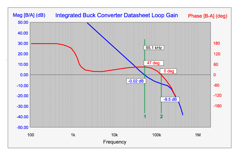
Figure 4: Semiconductor Manufacturer’s Loop Gain Example from Application Note
The loop example of Figure 4 shows a high loop crossover of 55.1 kHz with a measured phase margin of 47 degrees. While this is not an unreasonable design point, it should be recognized that the crossover frequency and phase margin will change significantly if the output capacitor is changed or the output inductor value is changed. It is also just one data point, and will vary with time, individual component choices, and temperature.
Injecting into the Loop
As these power supplies become smaller and smaller, it becomes increasingly rare to find a design where loop gain measurement is facilitated by the inclusion of test components and test points. Figure 5 shows what must normally be done to inject in the loop of the power supply. Feedback components shown in red must be lifted from the board, and the 20 ohm injection resistor shown in blue must be added, along with test leads to connect to with the measurement equipment.
If the board is laid out with testing in mind, and the components are of a reasonable size, this test is not particularly difficult to perform, and should always be included as part of the electronics assembly development.
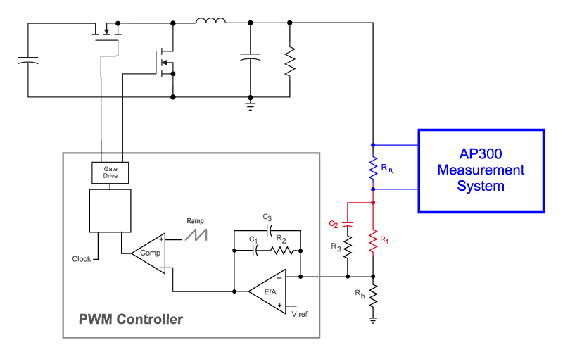
Fig. 5: Injecting Into the Loop. Components of the Feedback Must be Lifted From the Board, and an Injection Resistor Must Be Added. This is Not a Difficult Task When the Board Is Laid Out With Loop Testing in Mind.
Summary
The loop gain and phase provides a very sensitive measure of the relative stability of a power supply when coupled with its actual load and capacitors. Skipping this measurement misses the opportunity to find errors in design and identify power supplies which may be too close to the edge of instability. For modern point-of-load converters, recent technological developments have increased the risk of instability as performance is pushed to the edge of the envelope, making the measurements more necessary than ever.
References
- Join our LinkedIn group titled “Power Supply Design Center”. Noncommercial site with over 7000 helpful members with lots of theoretical and practical experience.
- For power supply hands-on training, please sign up for our workshops.
- Step-Load Testing [29-30],
http://www.ridleyengineering.com/design-center.html - Input Filter Interactions, Articles [60-62],
http://www.ridleyengineering.com/design-center.html - AP300 Application Notes and Videos
http://www.ridleyengineering.com/analyzer.html