


Point-of-load converters are prone to unusual results when considering the input filter design with low value capacitors.
Introduction
Point-of-load converters commonly use multilayer ceramic capacitors instead of electrolytic capacitors. The effect of this change is strongly felt in the bulk storage capacitor value, and can lead to unexpected variations in control measurements. Instability can result if input filter capacitors become too small.
Input Filter Closed-Loop Impedance Interactions
Figure 1 shows the schematic of a boost converter with a synchronous rectifier. It has multilayer ceramic capacitors on both the input and output of the converter. Since this is a boost converter, the capacitor on the output sees a pulsating current, and hence must be relatively large to keep the output ripple low. On the input side, the current ripple is small, and the input capacitor is typically chosen to be a smaller value.
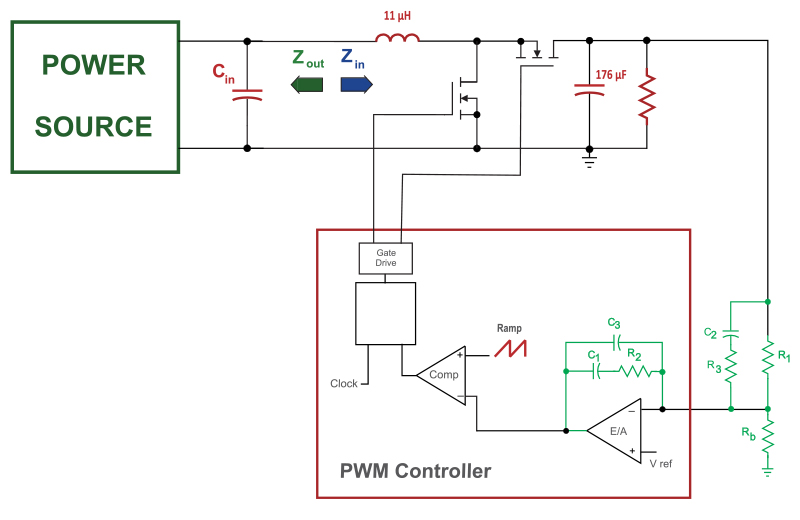
Figure 1: 200 kHz Boost Converter with Synchronous Rectifier and MLC Input and Output Capacitors
The input capacitance is important for a second reason. In addition to attenuating the switching ripple, it provides stability to the power system. If the impedance of the source providing the input voltage to a power supply becomes too large, the system can go unstable. The source impedance is formed by a combination of the upstream power supply output impedance, cabling impedance, and input bypass capacitors. Too low a value of capacitance will raise the impedance.
Figure 2 shows the output impedance of the power source using a capacitance of 88 µF directly across the input of the boost power supply. The ideal closed-loop input impedance of the boost converter is plotted on the same graph. A switching regulator with infinite bandwidth looks like a negative resistance, and Middlebrook’s famous work [1] on this topic pointed out that the output impedance of the input power source (or filter) must be lower than the closed-loop input impedance of the power supply if the system is to remain stable. It can be seen that this is true for the curves of Figure 2.
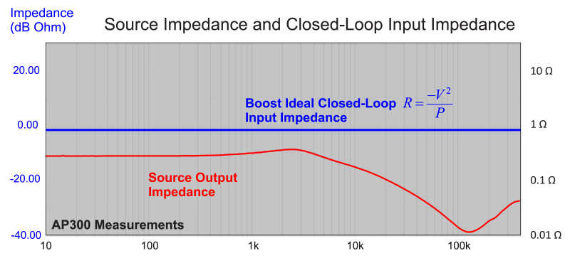
Figure 2: Output Impedance of the Power Source with 88 µF Versus Ideal Closed-Loop Input Resistance
Input Filter Open-Loop Impedance Interactions
Middlebrook also pointed out another important issue that is usually not given quite as much attention. If the output impedance of the input filter exceeds the open-loop input impedance of the power supply, the system won’t necessarily go unstable, but the transfer functions of the power converter will be changed significantly.
This aspect of Middlebrook’s work is not usually given as much attention since system designers often do not have the ability to open the loop of the power converter and measure the open-loop input impedance. In the past, this has not been a very significant oversight since the use of large bulk capacitances (needed to get low ESR) has naturally avoided impedance interactions. This changes with the switch to MLC capacitors.
Figure 3 shows the source output impedance overlaid with the measured open-loop input impedance of the boost converter of Figure 1. Since MLC capacitors are used on the output of the boost, the resonant dip in the input impedance is quite low. Its minimum value is limited only by the series resistance of the semiconductors and the inductor. It can be seen in this figure that there is a large area of overlap of the source output impedance and the power supply open-loop input impedance.
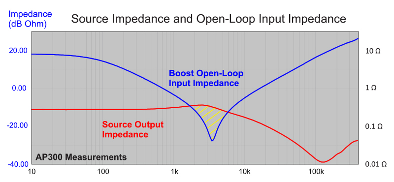
Figure 3: Output Impedance of the Power Source with 88 µF Versus Boost Power Stage Input Impedance
Figure 4 shows the control-to-output gain of the converter with the impedances of Figure 3. The transfer function is severely distorted in the frequency range where the impedances overlap each other. When you first encounter this type of measurement in the lab, it can be a surprise, and it looks like the converter is not working properly.
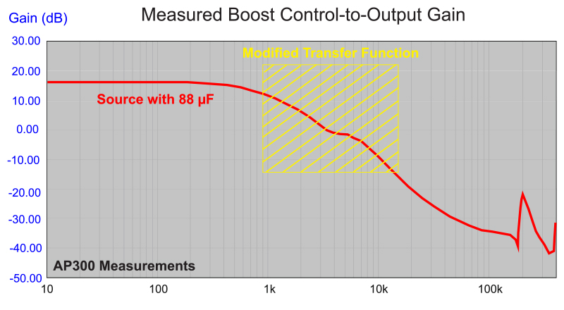
Figure 4: Control-to-Output Gain with 88 µF Input Capacitance. Notice the Distorted Transfer Function in the Region Where the Impedances Overlap
Reducing the Source Output Impedance
There are several design approaches possible when you encounter this kind of interaction. You can proceed with empirical measurements of the power supply to design the feedback loop, or you can construct more advanced modeling techniques to incorporate the effect of the impedance of the input filter. Vorpérian’s PWM switch model [2] works seamlessly with a source impedance to generate the proper transfer functions for you. You can do this either analytically, or within the framework of a circuit simulator such a Spice.
To some designers, it is important to avoid the open-loop impedance interaction problem altogether. With the interaction left in place, the transfer functions become analytically very cumbersome, and finding the worst-case operating point can be difficult.
The impedance interaction can be eliminated by reducing the source output impedance in the region of the power supply resonant impedance dip. Figure 5 shows the source output impedance with a 1000 µF capacitor added to the input of the boost converter. Now the source impedance is significantly lower, and there is very little overlap with the boost converter input impedance.
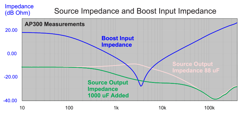
Figure 5: Source Output Impedance with 1000 µF Added Input Capacitance. Now There Only a Small Overlap with the Input Impedance.
Figure 6 shows the control-to-output measurement with the added 1000 µF bulk capacitance. The theoretical transfer function agrees well with the measured transfer function. Since there is still some impedance overlap, there is additional damping in the measurement.
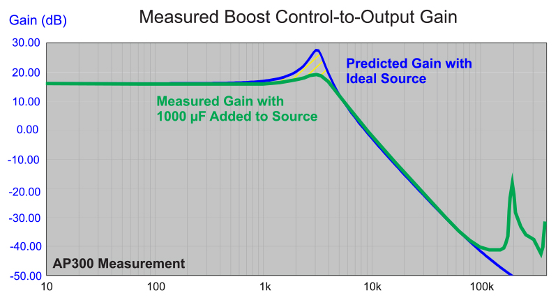
Figure 6: Control-to-Output Measurement with 1000 µF Added Input Capacitance. Theory and Measurement Agree Closely, Although There is Still a Discrepancy at the Resonant Peak of the Filter.
Effect of Source Impedance on Phase Response
The high source impedance of Figure 3 also has a very significant effect on the phase response of the control-to-output transfer function. µF The green curve of this figure shows the phase response with 1000 µF added to the system, and the red curve shows the response without this capacitor. Notice that there is a phase change of almost 60 degrees in the region just beyond the resonant filter of the power supply at about 4 kHz. This phase change can be problematic when embedding a board-mount power supply into a system.
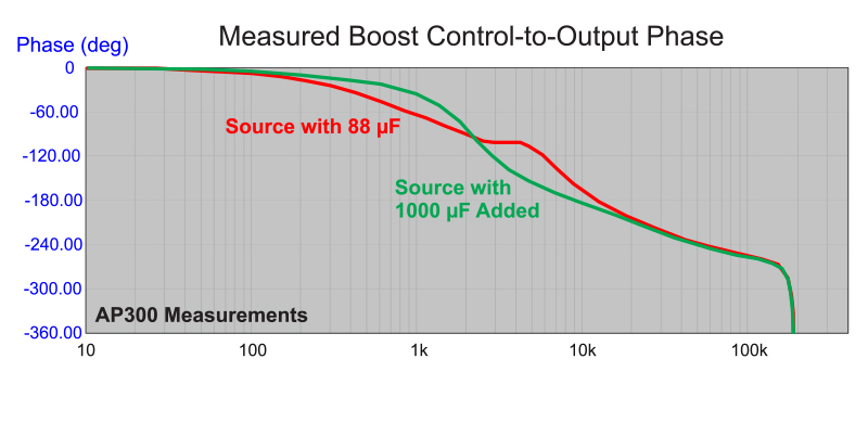
Figure 7: Control-to-Output Phase Measurements With and Without Added Bulk Capacitor
As was emphasized in [3], it is essential to measure board-mount power systems properly. At a glance, the converters may look like small linear regulators on the board, but their control characteristics are far more complicated. They have the extra inductor state in the feedback characteristics, and a negative input impedance which leads to the input filter problem discussed in this article.
Summary
When using only MLC capacitors on the input of board-mount power supplies, it is quite comment to run into Middlebrook’s filter interaction criteria. The resulting undamped systems make it quite likely that there will be an interaction with the open-loop input impedance of the power supply.
The interaction problem can be eliminated with the addition of bulk capacitance. If this is not possible due to the size of the capacitor, you can either extend modeling techniques to incorporate filter interaction, or you can depend on measurements to design the system. In either case, proper verification of the hardware loop gain measurement is essential to ensure system ruggedness.
References
- Join our LinkedIn group titled “Power Supply Design Center”. Noncommercial site with over 7000 helpful members with lots of theoretical and practical experience.
- For power supply hands-on training, please sign up for our workshops.
- “A New Small-signal Model for Current-Mode Control”, Raymond B. Ridley,1990 PhD dissertation, free download is available.
- Power 4-5-6 Design Software