Measuring input filter output impedance.
Introduction
In this article, Dr. Ridley continues the discussion of power supplies with input filters. He shows how the output impedance of the input filter is measured, and demonstrates the importance of input filter damping.
Input Filter Measurements
As discussed in the last article of this series [1], an input impedance measurement gives information about the characteristics of the power supply's input terminals. We use this information in conjunction with measurements of the output impedance of the input filter to assess whether a system interaction is likely to occur. This is important since it can lead to instability of the power supply control loop.
Figure 1 shows a block diagram of a switching power supply connected to an input filter. In order to assess filter interactions correctly, all filter components should be considered to be part of the input filter. This includes any bypass capacitors at the input of the switching power supply, and any other filter components that may be included at the front end of the power supply. In the last article of this series [1], the measurement of the input impedance of the power supply was demonstrated, and the effect of a small bypass capacitor was shown.
Fig. 1: Power supply with input filter module. All filter components, including input bypass capacitors, should be considered part of the input filter.
In this article, the techniques for measuring the input filter itself are presented. The output impedance of the filter can be measured as shown in Figure 2. The source from the frequency response analyzer is isolated through a wide-band transformer [2], and connected to the input filter in series with a current-sense resistor. If a 1-ohm resistor is used, no scaling is needed on the gain-phase measurement from the analyzer to convert to impedance values.
Fig. 2: How to measure the output impedance of the input filter. Notice the input of the filter must be shorted for a proper measurement.
The node between the sense resistor and the filter under test is connected to a ground reference. Channel A of the analyzer measures the voltage across the resistor (current signal) and Channel B measures the voltage across the filter (voltage signal). The ratio B/A of these two test signals gives the impedance of the input filter.
Notice that a short-circuit is placed across the input terminals of the input filter to properly make this measurement. Notice also that the filter impedance test is usually done without any power applied to the circuit. This greatly simplifies the setup and makes it a safe and straightforward test.
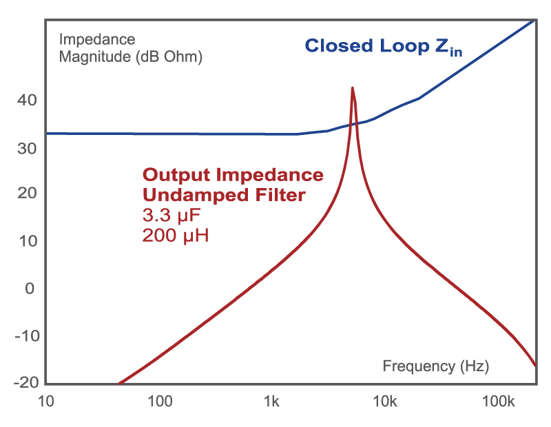
Figure 3 shows the results of impedance measurements for a switching power supply and the input filter.
Fig. 3: Comparison of measurements of power supply input impedance and input filter output impedance. With an undamped filter, the output impedance exceeds the input impedance of the power supply.
The blue curve of Figure 3 shows the closed-loop input impedance of the power supply, measured as described in [1]. The effect of the 3.3 µF bypass capacitor has been removed from this measurement, and this component is included in the filter measurements.
The red curve of Figure 3 shows the output impedance of the input filter with the 3.3 µF capacitor, and a 200 µH inductor. The capacitor has a very low ESR, and this produces a filter network with very little damping. At the resonant frequency of about 6.2 kHz, there is a very sharp peak in the output impedance, and its value exceeds that of the closed-loop input impedance of the power supply. There will be dramatic changes in the loop gain of the power supply, and this will be discussed in detail in the next article of this series.
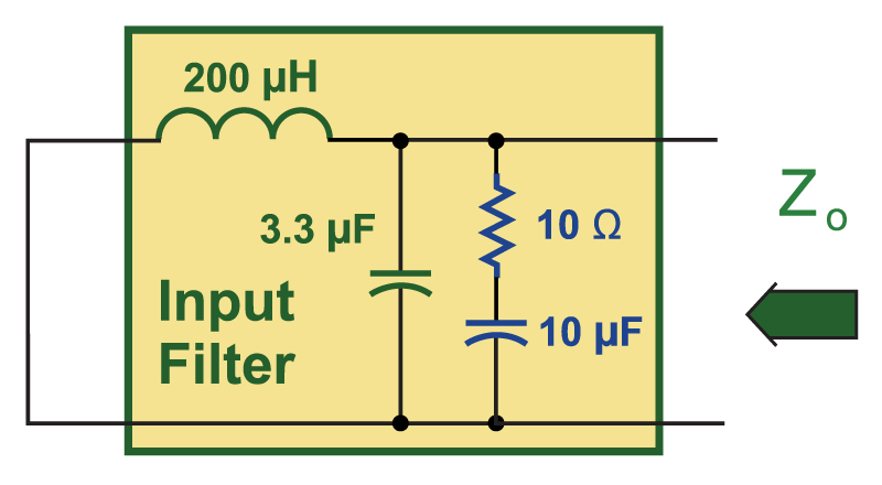
It is not advisable to have such an undamped filter at the input of the power supply, and the filter should be modified to avoid this. Figure 4 shows one possible network that can be used to damp this input filter effectively. A 10 µF capacitor in series with a 10 ohm damping resistor is connected in parallel with the original 3.3 µF capacitor. The new capacitor branch carries very little switching current and has minimal dissipation. (It is, however, a sizable component when compared to the 3.3 µF MLC capacitor.) This particular damping arrangement is chosen since it provides the same attenuation as the undamped filter at higher frequencies, and filter performance is not compromised for the sake of damping.
Fig. 4: One possible network for damping the input filter. This network applies damping at the filter resonance without affecting the attenuation or dissipation of the filter.
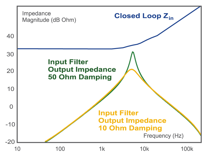
Figure 5 shows the effect of damping on the impedances of the power system. If a 50 ohm resistor is used, the output impedance of the filter is reduced to a value just a little less than the input impedance of the power supply. A 10 ohm resistor provides much better damping, and greatly reduces the Q of the input filter. This is a good design choice.
Fig. 5: Input filter impedance with added damping network.
The filter configurations used to meet conducted emissions standards of modern switching power supplies will be much more complex than the simple LC filter discussed here. However, damping networks can be applied in a similar manner, and the technique for measuring remains the same. Many power supply designers overlook the needs of damping the input filter, and often underestimate the amount of space needed for damping networks.
Summary
This article discusses how to measure and damp the output impedance of an input filter. This is a critical step for power supply design, and it must be done carefully. It is especially crucial for high density power supplies where capacitors have very small values of ESR, and high-Q filters are often created.
In the next article of this series, measurements of loop gains with and without the input filter in place will show the dramatic effects that result when the filter is not designed properly.
References
- Join our LinkedIn group titled “Power Supply Design Center”. Noncommercial site with over 7000 helpful members with lots of theoretical and practical experience.
- For power supply hands-on training, please sign up for our workshops.
- Ridley Engineering Design Center, "Input Impedance Measurements and Filter Interactions Part I"


