


PCB layout for the forward converter control chip.
Introduction
This article continues the series in which Dr. Ridley documents the processes involved in taking a power supply from the initial design to the full-power prototype. In Part IX, the second-generation of the PC board is described, and a critical area of layout is detailed.
Second Generation PCB
A second generation PCB was designed to accommodate errors in layout of the first pass board. This second design incorporated changes to component sizes where needed, and changes to the power supply specification. As described in the previous article of this series [1], a decision was made to attempt to provide four regulated outputs with a single supply after it was discovered that the real output power needed by the load was less than anticipated. This resulted in a major change to the magnetics, and testing of this concept was not possible on the first revision of the circuit board.
At each pass of the printed circuit board, the design should be made as complete as possible in order to move as close as possible to a production PCB. With major changes such as those encountered in this design, it is reasonable to anticipate as many as four iterations of the board design. The second iteration, shown in Figure 1, has many significant changes, and there may be some design issues to be tested and fixed with a further iteration.
Figure 1 shows the bare PCB with the major areas of the power supply. EMI filters are included on this board design, located close to the power entry and shown in red. The primary circuitry, also outlined in red, comprises the main input filter capacitor, and the two primary switches and clamp diodes. The power transformer and power inductor are shown outlined in blue. The new iteration of the power board has five outputs, using a coupled inductor. The layout of this region of the converter is particularly challenging, and will be described in a future article.
The control circuit is outlined in green in Figure 1. Bias power is supplied from an auxiliary power supply, and there is no direct connection between the control circuit and the primary of the power circuit.
A ground plane is located under the area of the control circuitry to provide quiet operation. More details of how ground and power planes can be used to improve the PCB layout for power supplies will be given in upcoming articles.
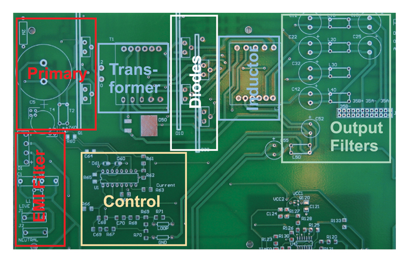
Figure 1: Second-pass PC Board Design
Control Chip Layout Critical Timing Capacitor Location
There is a common problem with the layout of power supply control chips, one that I see in many designs. Conventional PWM controllers use a current source to charge a capacitor, and then use the resulting ramp for the PWM modulator. The clock pin of these types of control chips is usually a very noise-sensitive part of the circuit.
It is crucial that the timing capacitor for the ramp be placed as close as possible to the PWM controller, and connected with very short traces to the pins of the chip. Figure 2 shows a circuit layout that did not work well. While the timing capacitor (on the bottom layer of the board) is close to the pins, the ground connection to the chip is too long. This resulted in significant noise on the clock, and the measurements of power supply transfer functions were severely affected by this noise. Some of the noise problems that can be exhibited by the clock are described in [2].
For this example, the long ground connection resulted from breaks in the ground plane, not from an intentional routing. This was overlooked in the first review of the board design.
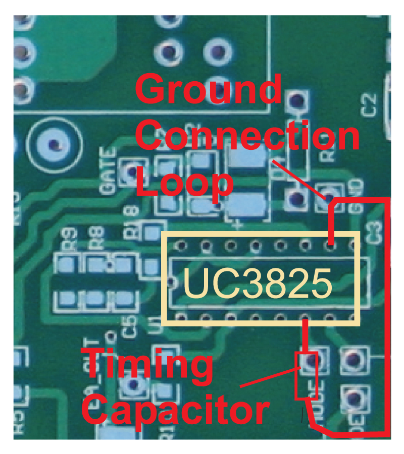
Figure 2: Detail of Control Chip Layout with Noise Problems
The importance of this part of the control circuit layout is paramount. In some cases, improper layout of this timing capacitor will directly lead to failure of the power supply. I have encountered this many times in my design career. The failure mechanism sometimes results from the clock working at very high frequencies during high-current operation, leading to overstress and failure of the power switch.
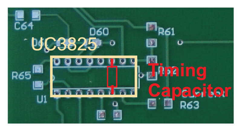
Figure 3: Detail of Control Chip Layout with Moved Timing Capacitor
Figure 3 shows a proper way to lay out this part of the circuit. The timing capacitor, shown in red, is located on the bottom of the circuit board, and connected with very short traces to the pins. With this arrangement, there are no clock noise problems, and control performance is very predictable and accurate.
Summary
Small details of PCB design can make or break a power supply. In this article, the detail of the layout of the timing capacitor is described. This is often the most crucial layout detail of the entire power supply. In following design tips article, other critical considerations for the board layout design will be described.
References
- Join our LinkedIn group titled “Power Supply Design Center”. Noncommercial site with over 7000 helpful members with lots of theoretical and practical experience.
- For power supply hands-on training, please sign up for our workshops.
- “Power Supply Development Diary Parts I - VIII”
- “Six Reasons for Power Supply Instability”