


PCB layout procedures including voltage spacing.
Introduction
This article continues the series in which Dr. Ridley documents the processes involved in taking a power supply from the initial design to the full-power prototype. In Part X, Dr. Ridley presents the rules for good PCB layout.
PCB Layout
In part IX of this series, an example was given of a crucial area of PCB layout around the control chip. This illustrated the details that need to be taken care of when laying out a switching power supply and its control circuit. Further examples of how to take care of specific issues on individual power supplies could take an entire book, something that is well beyond the scope of this design series. However, it is worth taking some time to highlight the important issues to be concerned with when laying out a switching power supply.
There are nine fundamental rules that should be followed for a switching power supply board.
Rule Number 1: Use at Least a 2-Layer Board
The cheapest possible power supplies use single-sided boards and jumpers where necessary. While this can be done, it makes a designer’s life extremely difficult. The preference is to use at least two layers. This provides much more design flexibility and a tighter, better performance and more rugged layout.
If working with more than two layers, it is advisable to keep critical power paths on the top and bottom layers where they can be clearly seen, and sometimes repaired in the event of failures during the development program. If inner layers are used, they should be properly spaced from each other, as discussed in Rule number 5 below.
Rule Number 2: Draw the Schematic Properly
There are several functions of a schematic: the first is to establish all connections properly for the CAD system, ready for the layout program. If schematic drawing is left in the hands of CAD designers with no power supply knowledge, this is the only thing that really matters to them. However, this ignores the other functions of the schematic.
A clear schematic of a power supply should clearly delineate the power stage topology, control circuits, and isolation areas. A quick glance at a schematic should be all that is needed to identify the type of technology being used for the power stage and control circuit. Many times, schematics are drawn in such a way that it is difficult to even identify which power topology is being used.
The schematic is also used to troubleshoot problems. Proper placement of components on the schematic should be logical relative to where they are placed on the board, and this speeds up the troubleshooting process.
Finally, the schematic should be used as a guide for showing the critical paths in the circuit, and should help you identify the crucial regions discussed in the layout considerations listed below. The schematic is the document on which you can sketch out the voltages, currents, and crucial paths, allowing you to think ahead about how the layout will be done.
Rule Number 3: Place All Power and Control Components Manually
Power and control components should be manually placed and oriented to facilitate the subsequent placement of traces. A proper schematic will show the appropriate components next to each other, and aid in the initial placement of the components. This work should always be done by someone with power supply design experience, and preferably by the engineer who is most familiar with the specific power supply being laid out. As the routing is done, it is not uncommon to change a component placement in order to optimize the layout.
Rule Number 4: Place Traces Manually
Experienced designers do not attempt to use autorouting for their power supply components. All critical power traces are placed by hand, allowing the designer to think about the optimal placement for minimizing EMI. Even the best modern CAD systems are inadequate for laying out switching power supplies automatically.
Rule Number 5: Use Proper Spacing for High Voltages.
A common mistake in the PCB design of many power supplies is inadequate spacing between traces, especially in the areas of the circuit where there are no specific agency rules that must be followed.
Figure 1 shows the forward converter schematic, simplified to a single output stage to illustrate the issues that arise with voltage spacing. The voltages that can exist on each trace are marked in different colors on this schematic.
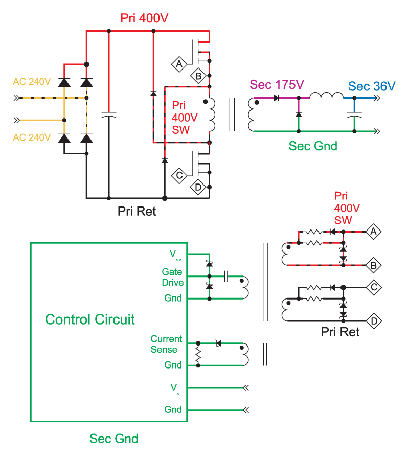
Figure 1: Simplified Forward Converter Schematic with Trace Voltages
Notice that there are multiple areas on the primary part of the schematic that can see up to 400 V, either DC, or with high-frequency switching. Careful attention must be paid to each of these areas in layout to prevent the possibility of voltage breakdown and failure in the power supply.
The secondary side of the circuit can also have high voltage potentials, especially at the output of the transformer. When assessing these voltage levels on your schematic, remember that you must include the high-frequency switching spikes that can occur, not just the anticipated square-wave voltages. Hence the voltage noted on the secondary of this converter is as high as 175 V.
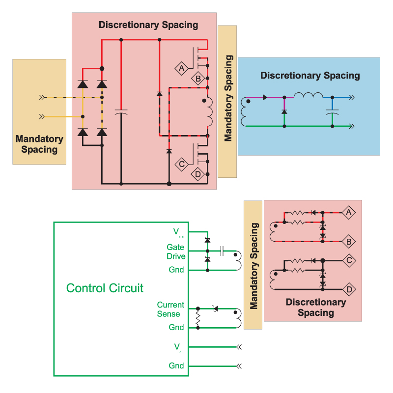
Figure 2: Simplified Forward Converter Schematic with Spacing Guidance
Despite the fact that high voltages exist at many points in a typical power supply design, there are surprisingly few hard rules for laying out a PC board. As shown in Figure 2, the safety agencies are only concerned with two areas on the board – the raw incoming AC power traces, and the separation of traces between the primary and safety-voltage secondary of the converter.
In these two areas of the converter design, there are very specific requirements for the distances between traces and component pads. On the primary side, with 240 VAC applied, the rules typically call out 2-3 mm of spacing, the actual number depending on the industry you are designing for. Free air has a typical breakdown rating of 1000V/mm, so this requirement provides plenty of margin.
Between primary and secondary circuits, the required spacing is even larger – typically 6 mm or more depending upon the particular application you are working on. It is very important that you clearly show this safety boundary area on your PC board, providing a clear path through all layers of the PCB. When held up to the light, the safety spacing should be apparent.
Once the input traces are separated from the AC input line by a component (which presumably can fuse for protection) there are no longer any safety requirements, and board spacing is strictly at the discretion of the layout designer. Also, on the secondary side of the converter, there are not any specific specifications for layout spacing.
Despite the lack of direct safety agency guidance, common sense should be applied to the parts of the circuit with high voltages between them. The 2-3 mm rule that is applied to the AC line exists for a reason – this extra spacing allows for nonideal situations such as condensation and contamination on the board. On the primary side, it is always a good idea to keep as much spacing as is reasonable, preserving the 2-3 mm if possible. For some power components, this is not always possible or practical, and the spacing must be compromised.
On the secondary side, also, do not immediately revert to CAD system minimum trace separations. You should always look at the actual voltages seen in the circuit, and space the traces and components accordingly.
Many companies have their own internal guidelines, and these should be followed carefully wherever possible. If your company does not have these, then common sense should prevail. If you have 1000 V between two traces, don’t put them just 1 mm away from each other. Even with conformal coating on a board, there is usually no reason to make the spacing so small.
Figure 3 shows an example of a pre-production power supply where discretionary spacing issues were ignored on the PCB layout. The mandatory rules were adhered to in the primary spacing, and the safety spacing areas, so the board would pass agency inspection. However, in this example, some of the discretionary spacings are so small that breakdown of air is possible even though the initial prototypes worked fine. This particular board was modified before production to increase the crucial spacing areas.
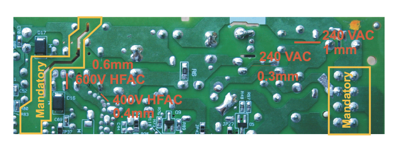
Figure 3: Example Preproduction Power Supply Board with Inadequate Spacing.
In reviewing power supply designs over the last couple of decades, I have seen this to be a very common error. Modern tiny packages have exacerbated the issue. Another insidious problem that can exist is when inadequate spacing is provided between high-voltage traces on inner layers of a PCB. Inexperienced designers may be counting on the insulation of layers for protection, but lateral failures can occur on inner layers if insufficient spacing is used.
Summary
There are nine basic rules for laying out a PCB for switching power supplies. Five of them have been covered in this article, with special attention applied to the proper voltage spacing between PCB traces. The remaining four rules, involving the routing of traces, and placement of planes, will be covered in the next article of this series.
References
- Join our LinkedIn group titled “Power Supply Design Center”. Noncommercial site with over 7000 helpful members with lots of theoretical and practical experience.
- For power supply hands-on training, please sign up for our workshops.
- “Power Supply Development Diary Parts I-IX”