


PCB layout procedures including current loops.
Introduction
This article continues the series in which Dr. Ridley documents the processes involved in taking a power supply from the initial design to the full-power prototype. Part X of this series of articles presented the first five rules for good PC board layout. Part XI concentrates on the sixth and seventh rules, which are concerned with the routing of high-frequency currents.
PCB Layout Rule 6: Keep High-Frequency Current Loops Small
Switching power supplies generate high-frequency waveforms with both high-current and high-voltage pulses. These waveforms generate a broad spectrum of frequency components for square-wave converters. If the PC board is not laid out properly, the high-frequency currents can create numerous problems, including large stray inductances with associated energy storage, increased component stresses, and EMI issues that are very difficult to suppress.
These problems can be controlled by following the sixth rule of good PCB layout: Keep high-frequency current loops as small as possible. This requires careful thought regarding circuit functioning and board layout.
Figure 1 shows the basic schematic of the forward converter with a single output. When the power switches are turned on, a high-frequency pulse of current flows through components C1, T2, Q1, T1, and Q2. A corresponding pulse of current flows through the secondary of the transformer, and the forward diode.
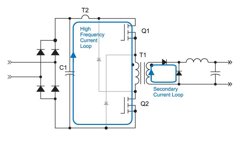
Figure 1: Forward Converter Schematic with High-Frequency Primary Current Path
It is important that the loop containing these components presents a low inductance. Figure 2 shows the placement of the primary components, and a preliminary layout of the board. In this example, all of the traces are placed on the upper layer and shown in red. This facilitates the testing of the power supply, and is useful for a single-sided board. Attention has been paid to ensure that the traces are well separated for voltage breakdown considerations.
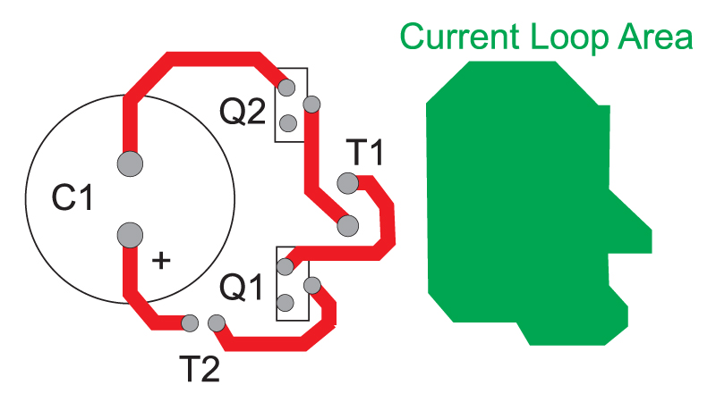
Figure 2: Forward Converter Primary Component Layout on a Single Layer.
However, the layout of the primary in this example creates a large current loop area, shown in green. This large area results in increased inductance, and a single turn antenna that will radiate EMI that is difficult to suppress. The severity of the problem will depend upon the current levels. Even at low power and current levels, however, these large-area current loops should be avoided.
A similar problem exists on the secondary side of the transformer. For step-down converters, secondary currents are higher and the layout of the secondary is even more crucial. The issues are the same. The illustration of secondary layout is not shown in this article.
Figure 3 shows how the primary layout can be improved by using both layers of the PC board. In this case, the top (red) and bottom (blue) layers are used to carry opposing currents, thus providing cancellation of magnetic fields. This is the optimal situation from the standpoint of minimizing inductance, energy storage, and EMI. To achieve this, some of the board spacings are not as large as we would like to see.
Also, the presence of multiple traces on both layers restricts the flexibility of component placement on the underside of the board. This will impact the performance of other parts of the primary circuit, specifically the effectiveness of the clamp diodes.
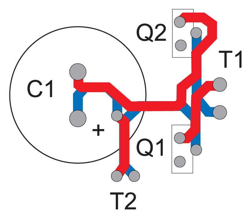
Figure 3: Forward Converter Primary Layout on Two Layers.
Figure 4 shows an alternate arrangement where there is a compromise between minimum loop area, keeping the bottom layer of the board mostly free of traces. In this case, there is at least a 4:1 reduction in current loop area compared to the first layout, while maintaining acceptable voltage spacing.
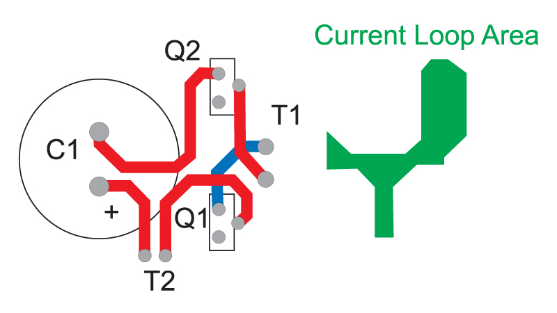
Figure 4: Primary Layout with Small Loop Mostly on Top Layer.
The layout of Figure 4 now lets us design a good layout for the next phase of the primary operation, shown in Figure 5. When the power switches turn off, the primary current flows through the two diodes. One purpose of these diodes is to reset the magnetizing current in the primary of the transformer. This is a relatively low current. However, the diodes also provide a clamp for the power devices, and the path through these diodes must be kept as short as possible to avoid excessive voltage spikes caused by the transformer leakage inductance. Proper layout of these parts saves us having to use additional bypass components on the primary of the converter.
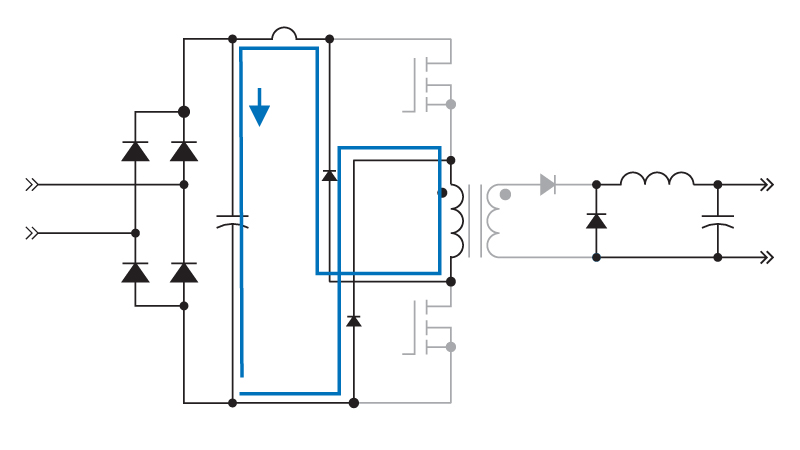
Figure 5: Forward Converter Schematic with High-Frequency Primary Diode Current Path
Figure 6 shows the placement and traces for the clamp diodes. The previous top and bottom traces are now shown in grey for clarity, and the diode traces and pads are on the bottom of the board in blue.
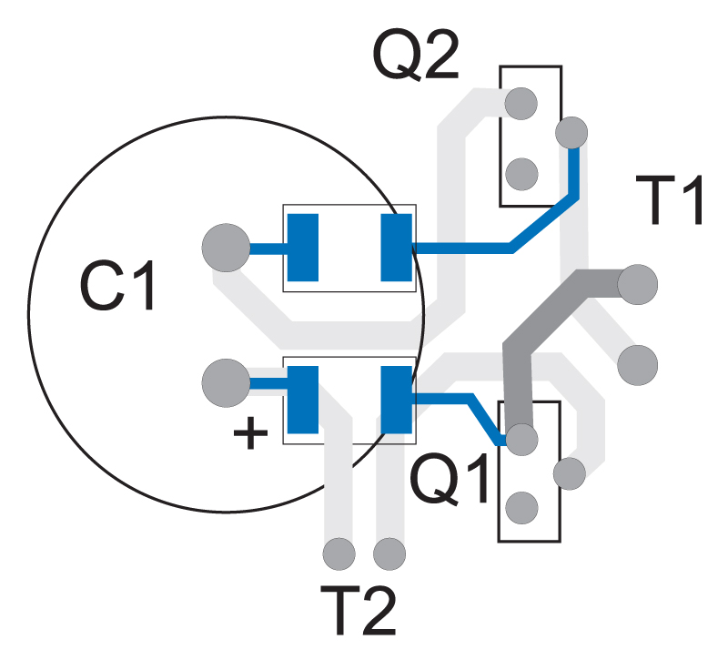
Figure 6: Primary Clamp Diode Layout.
Layout Rule 7: Show the Currents Where to Flow
In closing the current loops as shown so far, we are also following Rule Number 7 of good layout: Show the currents where to flow. The high-frequency currents of a converter must be given only one path to follow to ensure predictable performance. In some cases, there may be multiple connections to a circuit node, but the high current paths must be explicitly laid out.
An example of this is shown in Figure 7 for the gate drive connections to the primary power switches. Gate drive layout is important for several reasons. Firstly, high currents are sometimes needed to switch FETs rapidly, and these can create EMI if the current loops of the gate drive are not closed. Secondly, it is important that the main power currents do not affect the gate drive waveforms due to poor layout.
In Figure 7, it is shown that the returns of the gate drive traces go directly to the source of the power FETs, and not to some other part of the same circuit node. This prevents the power currents from flowing through the gate drive circuit.
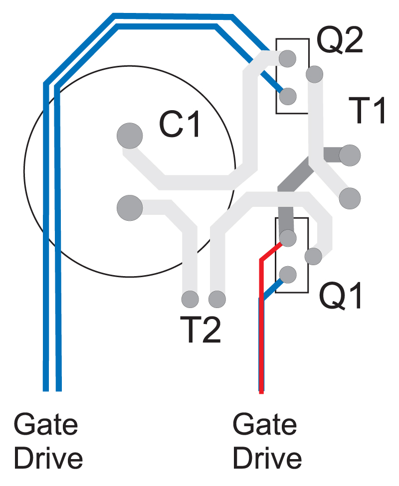
Figure 7: Primary Gate Drive Layout.
Ideally, the gate drive signals flow on opposite sides of the PC board. However, with a two-layer board, this is not always possible. In Figure 7, the left hand gate traces are both on the bottom of the board, but with small separation since there is not a large voltage differential between the traces.
Summary
The last few articles have shown seven of the nine critical rules for good PC board layout. Considerable time must be spent on the board layout as this can eliminate later problems with component stresses, proper circuit operation and EMI. The engineer who is intimately familiar with every detail of the circuit operation must be closely involved with the actual board layout, down to the very detailed placement of parts, and proper routing of traces to satisfy multiple simultaneous requirements. This is not a process that can be left to a PCB designer without power experience.
In the final part of this series regarding PCB layout, the proper use of ground and EMI shielding planes will be discussed.
References
- Join our LinkedIn group titled “Power Supply Design Center”. Noncommercial site with over 7000 helpful members with lots of theoretical and practical experience.
- For power supply hands-on training, please sign up for our workshops.
- “Power Supply Development Diary Parts I-X”