


PCB layout rules for use of ground and other planes.
Introduction
This article continues the series in which Dr. Ridley documents the processes involved in taking a power supply from the initial design to the full-power prototype. Parts X and XI of this series of articles presented the first seven rules for good PC board layout. Part XII finishes up the design rules for good PCB layout design, focusing on the judicious use of planes.
PCB Layout Rule 8: Use Planes to Capture Noise
Switching power supplies generate high-frequency waveforms with both high-frequency and high-amplitude current and voltage pulses. In the last article of this series, it was shown how to keep current loops small in order to minimize leakage inductance and magnetic EMI generation. This is an essential step since shielding of magnetically-generated noise is difficult. It is better not to generate it in the first place, hence the need to close the high-frequency current loops.
Noise is also generated by electrostatic antennae created by the power supply components. Nodes which have high-frequency voltage waveforms, when coupled with large-area components or heatsinks, will generate considerable amounts of EMI.
Figure 1 shows the basic schematic of the forward converter with a single output. The worst electrostatic noise generators are shown in blue, red, and purple. These are the nodes of the circuit with the highest dv/dt waveforms. Typically, the waveform shown in red is the worst offender since it is tied to the large surface area of the drain of the lower power FET.
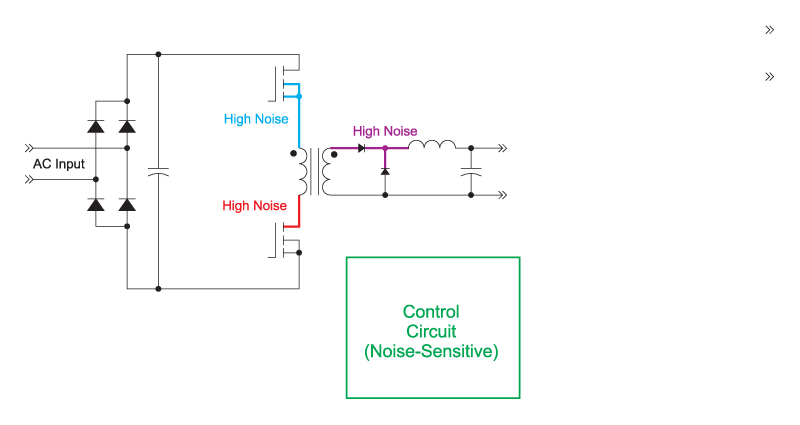
Figure 1: Forward Converter Schematic showing Electrostatic Noise Generators
Shielding planes can be used to greatly reduce the effect of these noise-generating nodes. Three such planes are shown in Figure 2. These can be implemented in the PC board, if space and available layers allows, and if the power components are surface mounted. The planes should be tied to local RF ground points, such as the return of the main power rail on the input, or the return of the output voltage.
Notice that there is no plane for the source of the upper FET since this is normally self-shielding due to the layout of the power packages. The substrate of most FETs are connected to the drain of the FET. The upper FET is connected to an RF ground point on the positive side of the input rail.
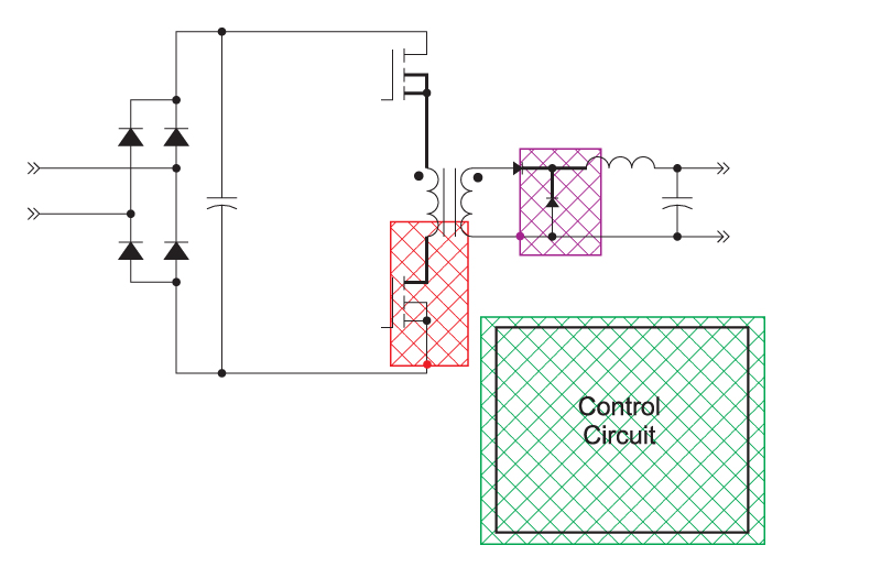
Figure 2: Shields for Collection of Electrostatic Noise (Red and Purple) and for Control Circuit Shielding (Green). Colored Dots Show Where Shields are Connected.
If the power components are through-hole mounted, the use of planes to collect EMI in the PCB will be of limited value. In this case, the heatsinks of the power components themselves should be locally grounded, ensuring that they have suitable voltage isolation from the power devices.
Layout Rule 9: Use Planes to Shield from Noise
PWM controllers can be very sensitive to noise, and must be protected to ensure proper operation. Stray noise into the ports of high-gain operational amplifiers and comparators can lead to catastrophic failures of power supplies. Even the simple act of applying an oscilloscope probe improperly to a control circuit can result in failure of a switching power supply.
It is highly advisable to provide a ground plane underneath the area of the control chip and its surrounding components. This will establish a low-impedance ground connection to all parts of the control circuit, and minimize any EMI pickup loops and stray inductance that may cause problems. The ground plane used to shield the control circuit should be tied properly to the return of the main output if this is referred to the same ground. A single connection should be provided to connect the two common points as shown in Figure 3.
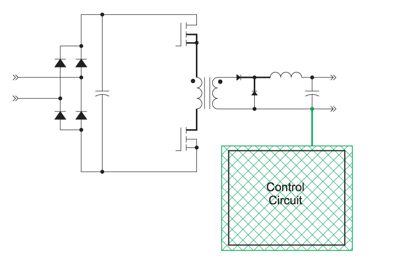
Figure 3: Tying the Ground Plane to a Single Point on the Main Output
If extra layers are available on the PCB, it can be tempting to pour a ground plane over much larger areas in order to reduce noise. However this can have the effect of degrading the integrity of the ground in the quiet areas of the circuit. For example, if a ground plane is placed on the PCB as shown in Figure 4, noise problems can result. The high-frequency pulsating currents in the secondary will flow through parts of the ground plane, and this can disturb noise-sensitive components.
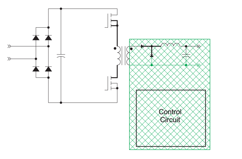
Figure 4: Using a Single Ground Plane can Degrade Ground Integrity
A better layout for ground planes is illustrated in Figure 5. The upper part of the plane is used for two purposes – first, to shield the electrostatic noise generated by the output rectifiers (shown in purple in Figure 1), and secondly, to provide a large conduction area for the ground of the output with low impedance.
The lower part of the plane is used just to keep the noise from interfering with the control circuit. None of the high-frequency or high-current waveforms are allowed to flow through this part of the ground plane. This preserves the integrity of the ground. The two separate parts of the plane are connected by a single trace on the PCB.
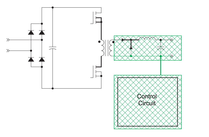
Figure 5: Two Separate Ground Planes Achieve Noise Shielding and Proper Ground Integrity
Layer Choices for PCB Planes
If you have two or more layers on the PCB, you have choices as to where to put the shielding planes. There are several design philosophies that may be used in choosing where you put the plane layers.
I always like to have access to all the trace routings in order to be able to see all of the waveform nodes, and sometimes to make changes on the early iterations of the PCB. For complicated boards, this can tie up the top and bottom layers of the circuit board, requiring the ground and shield planes to be placed internally. With simpler circuits, most of the traces can often be placed on one side of a double-sided board, leaving the other free for planes.
Another convenient choice is to put the ground plane under the control circuitry on the top layer of the PCB. This provides a local ground connection for probing the circuit with short lead lengths. If you are using SMT components, you will not be able to put a plane on that same layer if the component density is high.
The resulting compromise solution is to place each plane individually, taking care of functionality and practical aspects at the same time. There is no single optimal solution for every design. Think carefully about the role of each part of a plane. With a two-layer board, a good solution can usually be found.
The outline of the planes should be placed on the board manually, thinking carefully about the components that need to be shielded from either generating or being susceptible to noise. Once the CAD system has filled in the area of the plane, ensure that all parts of the plane are properly connected and that isolated islands and long connections have not been inadvertently generated. Occasionally, traces will need to be rerouted to keep the planes reasonably intact.
It is important not to just pour planes across the entire expanse of the board, even if the layers and space are available. Planes that are designed to protect sensitive circuits should not be continued in the areas where there are noisy components, or they may do more harm than good.
Summary
The last few articles of this series have shown the nine critical rules for good PC board layout. The last step, placing power and ground planes for EMI control, is a process that involves intimate knowledge of the operation of the power circuit, and cannot be automated. It takes a lot of experience to do this effectively.
Following these nine critical rules will help achieve good results on your first boards. Laying out a good circuit board for power supply design is a skill that takes years to acquire, and the time-consuming nature of this task should never be underestimated. With each new power supply design, anticipate at least two iterations of the PC board. This is true even if there are no changes to the circuit schematic.
If you are new to power supply design, it is highly recommended to begin to learn the art and science of power supply board layout as early in your career as possible. This is a very valuable skill that will greatly increase effectiveness as a power designer
References
- Join our LinkedIn group titled “Power Supply Design Center”. Noncommercial site with over 7000 helpful members with lots of theoretical and practical experience.
- For power supply hands-on training, please sign up for our workshops.
- “Power Supply Development Diary Parts I-XI”