


Dr. Vorperian's analysis of the tightly-coupled sepic converter.
Introduction
This article gives the analytical transfer function for the tightly-coupled Sepic converter. It is shown that the control-to-output function is just second-order, not fourth-order like the conventional Sepic converter [1]. The coupling capacitor of the converter has no effect on the control, and it can be made small.
Coupled-Inductor Sepic Converter
Figure 1 shows a Sepic converter with coupled inductors. In general, the coupled inductors would be wound on a single core with significant leakage between them. This allows for substantial reduction of the input ripple current of the converter by tuning the relative values of the inductances. However, recent trends have shown manufacturers are providing tightly-wound inductors, with very low leakage, and a 1:1 turns ratio. Even when the inductors are tightly coupled in this, performance of the converter is good. As shown in [2] the ripple at the input of the converter is reduced from the non-coupled inductor design. It will be shown later that the tight coupling reduces the complexity of the converter control characteristics.
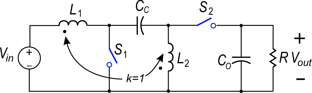
Figure 1: Coupled-Inductor Sepic Converter Circuit with Switches
The Sepic converter is popular since it can provide either step-up or step-down, and a non-inverted output without using a transformer in the circuit. It was shown in [2] that the tightly-coupled inductors lead to a fairly benign transfer function for the control-to-output, eliminating the complex 4-th order characteristics of the regular Sepic converter. While measurements were made in [2], no analytical expressions were provided to confirm the relative simplicity of the converter.
In order to perform analysis on the Sepic converter using the techniques described in [3] we must first rearrange the circuit to show the location of the PWM switch. This step is shown in Figure 2: the second inductor is moved on the diagram, while keeping each end of the inductor connected to the same nodes in the circuit. The second switch is also relocated, from the right of Cc to the bottom leg of the circuit. The resulting configuration maintains the exact same function of the original Sepic circuit. Once this is done, you can clearly see the location of the PWM switch model, so analysis of the circuit will be straightforward.
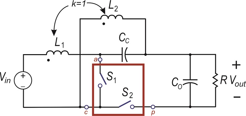
Figure 2: Rearranged Sepic Converter Reveals the PWM Switch Model
Figure 3 shows how the coupled inductors are now replaced with a conventional transformer model, consisting of an inductance and an ideal transformer. Since the coupling is ideal, no leakage inductance is included in the model. We can see immediately the circuit order is reduced from four states to just three since only one inductor is needed in the transformer model. The operation of the transformer will then also eliminate another state, Cc, and this will show up in the final transfer functions. When the switch is turned on, the input voltage Vin is applied directly to the capacitor Cc, and its voltage is not allowed to move.
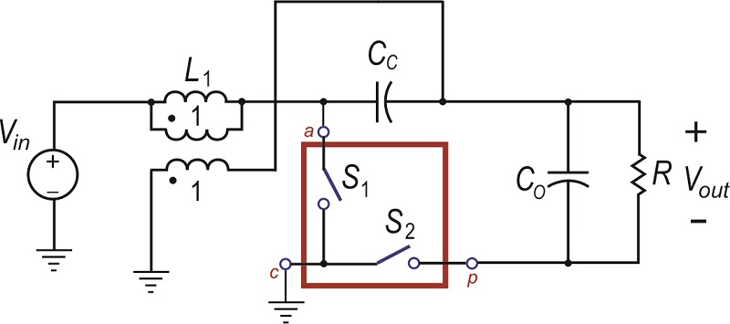
Figure 3: The Tightly-Coupled Inductors Replaced with a Transformer Model
The final step before applying circuit analysis techniques is to replace the two switches of the PWM switch model with its small-signal equivalent circuit model. This step is shown in Figure 4. We now have a linear, small-signal circuit where we can apply standard circuit analysis techniques to derive any of the desired transfer functions. Normally, we would derive the input impedance, output impedance, line-to-output, and control-to-output transfer functions to completely characterize the converter. In this article, we concentrate just on the control-to-output transfer function.

Figure 4: Small-Signal Linear Circuit Model Ready for Hand Circuit Analysis
Control-to-Output Transfer Function Result
Figure 5 shows the control-to-output transfer function that results from the analysis. You can see that the expression is quite simple. There is a double pole in the transfer function, and a single RHP zero. The dc gain, Kdc, is the same as the regular Sepic. As the input voltage to the converter is increased, the dc gain actually decreases. This is a characteristic that is also shared by the boost and flyback converters.
Notice that the coupling capacitor, Cc, has no effect on the control characteristic at all. The capacitor can be quite small, just large enough to carry the required rms ripple current of the converter. There is no need for this capacitor to have any significant energy storage, which is a considerable space savings for dense converter design.
Like the boost and flyback converters, the resonant frequency of the control transfer function is a function of the line voltage, and corresponding duty cycle. The inductor value is effectively modified by the duty cycle of the converter. At low line, the resonance will have its minimum value.
The control transfer function also has a right-hand-plane zero. The value is determined by the output loading and the inductor value, plus the input line (or duty cycle.) At low line and full load, like the boost converter, the RHP zero has its lowest value. Typically, the maximum allowable crossover frequency will be about 1/5 of this RHP zero frequency, so this limits the control performance.
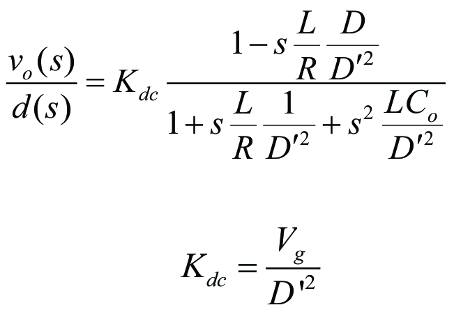
Figure 5: Resulting Control Transfer Functions for the Tightly-Coupled Sepic Converter
In [1], the coupled-inductor Sepic was built and measured. The worst-case phase delay, as predicted by the first expression in figure 5, is -270 degrees. This is verified by the measurements of Figure 6. It can be seen that the model is indeed just 2nd order, with a single RHP zero. The difficult control characteristics of the full uncoupled Sepic converter are made manageable by the coupling of the inductors. A pair of complex RHP zeros and complex double poles are completely eliminated by the couple magnetics.
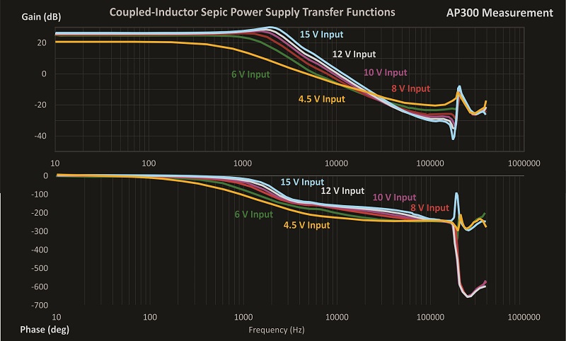
Figure 6: Measured Control Transfer Functions for the Tightly-Coupled Sepic
The only remaining complexity is the RHP zero, and this can easily be managed by choosing a smaller value of the inductance. The smaller this value, the faster the inductor current can be changed by the control, mitigating the effect of the RHP zero.
Summary
The control-to-output transfer function of the coupled-inductor Sepic converter has been derived. It has a single RHP zero, and a double pole. The coupling capacitor value does not affect the control transfer function, and hence the capacitor value can be chosen to be quite small. The control-to-output transfer function derived in this article should prove very useful to all designers of this converter.
References
[1] “[S01] Sepic Converter Analysis Notes”, Dr. Vatché Vorpérian.
[2] “[81] Sepic Converter Measurements - Part II Coupled Inductor Design”, Power Supply Design Center.
[3] “Fast Analytical Techniques”, Dr. Vatché Vorpérian,
[4] AP300 Application Notes and Videos,
[6 Join our LinkedIn group titled “Power Supply Design Center”. Noncommercial site with over 7100 helpful members with lots of theoretical and practical experience.
[7] See our videos on loop testing and power supply design
[8] For power supply hands-on training, please sign up for our workshops at http://www.ridleyengineering.com/workshops.html