Frequency Response
-
[002] Sepic Converter Analysis
The Sepic converter dc analysis is presented, showing why this is a popular converter. Beware of the ac characteristics though.
Introduction
In the last article, we talked about the simplest of all converters, the buck converter, and showed how its control transfer functions could be extraordinarily complex. In this issue, we’ll go to the other end of the spectrum, and look at a converter that is far more complex, yet is often used by engineers who are unaware of the difficulties they may be in for.
Call this article, if you like, part II of “Power Supplies are Supposed to be Easy!”
The Sepic Converter
The most basic converter that we looked at last month is the buck converter. It is so named because it always steps down, or bucks, the input voltage. The output of the converter is given by

Interchange the input and the output of the buck converter, and you get the second basic converter – the boost. The boost always steps up, hence its name. The output voltage is always higher than the input voltage, and is given by:

What if you have an application where you need to both step up and step down sometimes, depending on the input and output voltage? Well, you could use two cascaded converters, one a buck and one a boost. Unfortunately that needs two separate controllers and switches. (It’s actually a good solution in many cases, and should not be rejected out of hand.)
The buck-boost converter has the desired step up and step down functions

but the output is inverted. A flyback converter (isolated buck-boost) requires a transformer instead of just an inductor, adding to the complexity of the development.
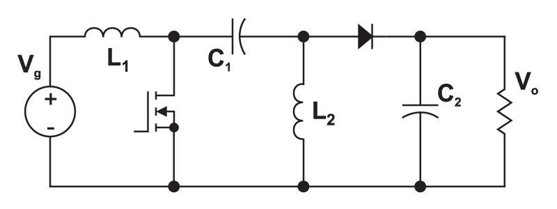
One converter that provides the needed input-to-output gain is the Sepic converter (single-ended primary inductor converter). This is shown in Fig. 1. It has become popular in recent years in battery-powered systems which must step up or down depending upon the charge level of the battery.
Figure 1: The Sepic converter can both step up and step down the input voltage, while maintaining the same polarity and the same ground reference for the input and output.
Fig. 2 shows the circuit when the power switch is turned on. The first inductor, L1, is charged from the input voltage source during this time. The second inductor takes energy from the first capacitor, and the output capacitor is left to provide the load current. The fact that both L1and L2 are disconnected from the load when the switch is on leads to complex control characteristics, as we will see later.
-
[004] HF Transformer Measurement and Modeling
How to measure and model high-frequency magnetics for switching power supplies. Essential steps for both custom-designed parts, or purchased components.
Power Supply Design Tips
This article points out some of the issues involved in designing, measuring, and modeling high-frequency magnetics for switching power supplies.
Despite efforts from some magnetics vendors to provide off-the-shelf components to power supply designers, almost all high-performance magnetics are custom. There are many deep and complex issues involved in the design of magnetics. I will try to cast some light on just a few of these issues.
Transformer Design Example
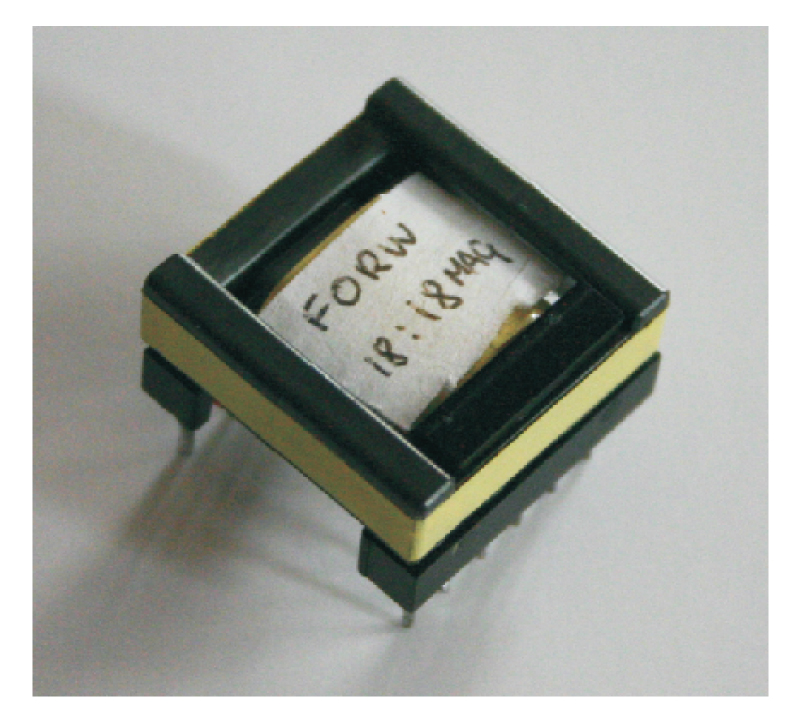
Figure 1 shows a simple 1:1 transformer. The transformer uses an ungapped EPC-25 core from TDK, made from PC-44 material. This transformer was designed for use in a 60 W forward converter with 36-60 V input and 12 V output.
Figure 1: A simple 1:1 transformer designed for a 100 kHz, 60 W forward converter.
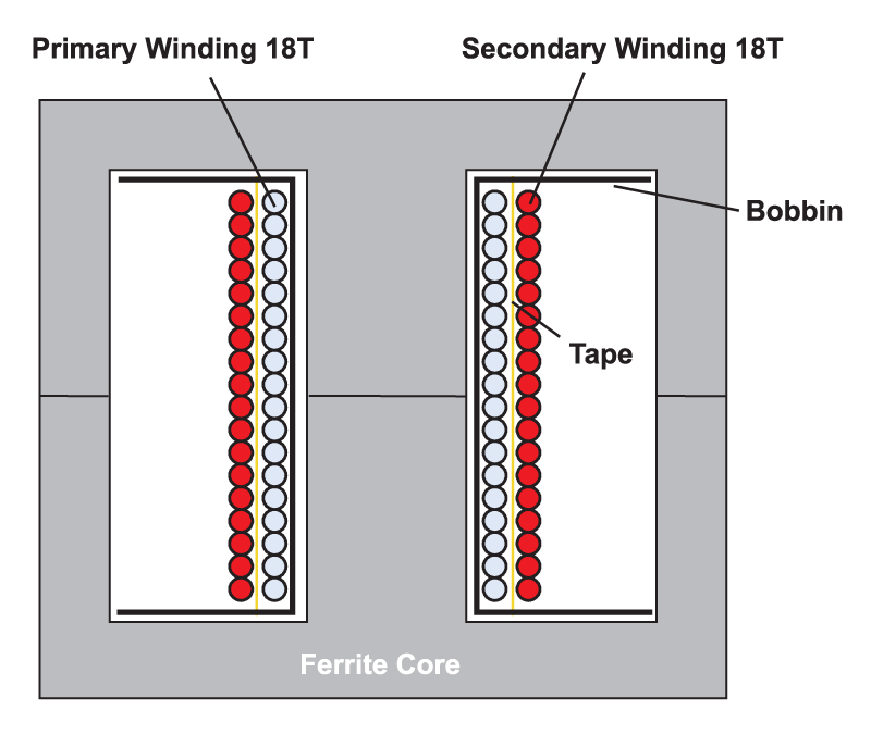
Figure 2 shows the winding layout, with just a single layer of 18 turns for the primary winding, a layer of thin insulation tape, and a single layer of 18 turns for the secondary winding.
Figure 2: Winding layout of the transformer of Figure 1.
This is a very straightforward, easy-to-manufacture design of a two-winding transformer. However, as you will see below, the resulting circuit element created is anything but simple.
-
[005] High Frequency Power Inductor Design
Proximity Loss in Magnetics Windings
Exploring the use of custom versus off-the-shelf magnetics design. Standard parts are designed to a price point, and must be tested properly if you want to use them.
Power Supply Design Tips
In this article, we continue the theme of custom versus off-the-shelf magnetics design. The relatively simple output inductor of a forward converter is used as an example to show the issues and pitfalls involved in trying to use off-the-shelf inductor designs for high-frequency power supply applications.
Power Inductor Design
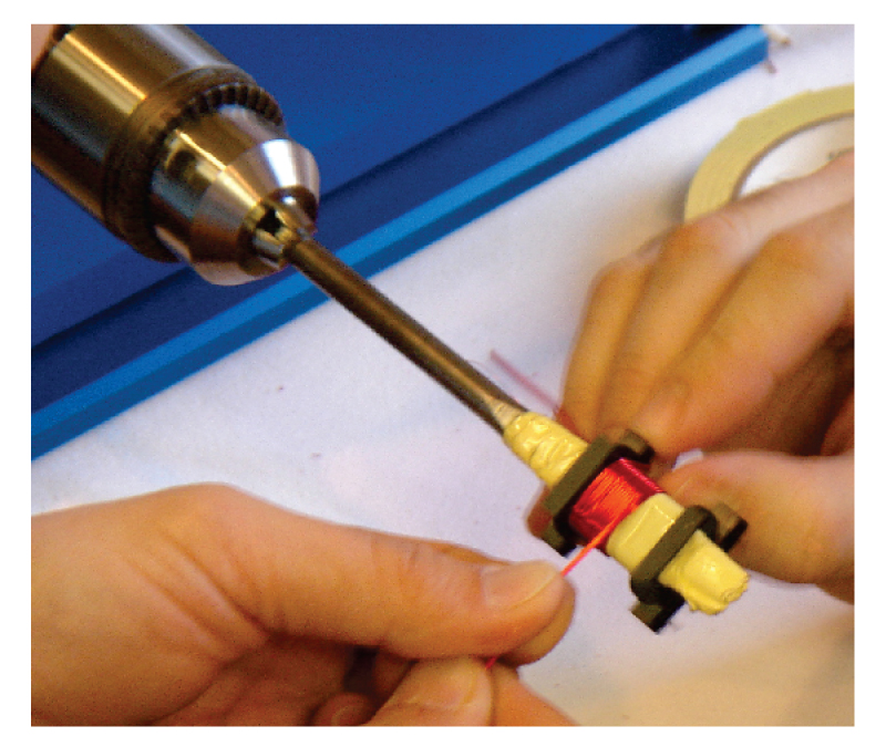
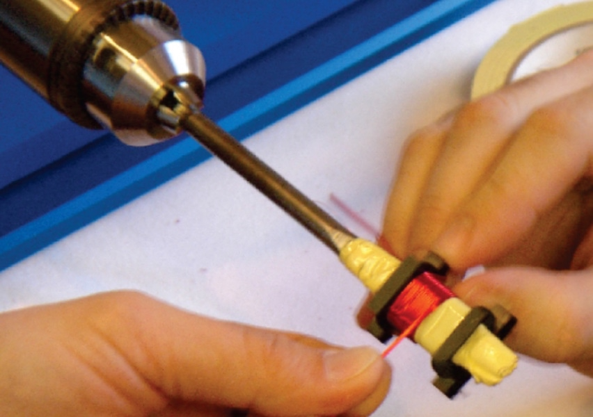
When I first started my career in power electronics, over 25 years ago, all magnetic components were custom designed and manufactured. In our current power supply design workshops, we dedicate an entire day to the theory and practice of making custom inductors for switching power supplies. Attendees at the course design, analyze, and build their own inductors and transformers in the lab.[1]
Figure 1: Building custom magnetics in our design workshop.
In the last few years, numerous companies have developed kits of standard parts aimed at the semiconductor companies to integrate into their designs. This proliferation of parts has recently led me to wonder if custom inductor design was becoming a skill belonging more to the past than the future.
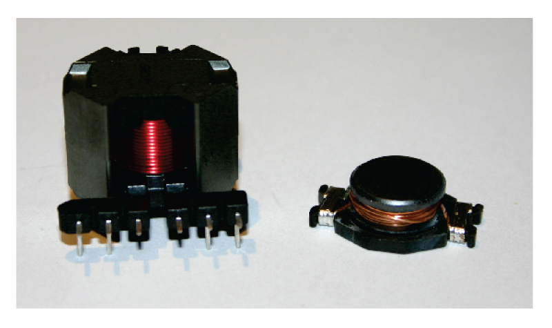
Figure 2 shows two inductor designs, one developed in our workshop for a rugged 60-W converter, and the smaller low-cost, off-the-shelf part. You can see a significant size advantage of the standard component.
Figure 2: (a) 47 µH custom inductor and (b) off-the-shelf commodity component
The 47µH custom inductor was designed to operate continuously at 5 A, with plenty of margin for overcurrent situations.
The off-the-shelf inductor, also 47µH, had a single number assigned to it on the parts kit—a current rating of 5 A. Since the parts kit is aimed at the non-experienced power supply designer, it seems reasonable to assume that the inductor is suitable for a 5 A converter application
The parts are quite different in their design, as shown in Fig. 3. The custom-made inductor has a single-layer winding on an RM8 core, with a gapped center leg. The windings are a significant distance away from the center leg gap, essential to avoid proximity losses in the windings at high frequencies.
-
[006] The Digital Power Supply Revolution

Digital power is all the rage now, but don't expect it to shorten your design time, or to eliminate the need for complete optimization of the analog parts of the power supply.
Introduction
At the recent Applied Power Electronics Conference, digital power supplies were featured everywhere, in papers, seminars, and poster sessions. Applications were widespread, in VRMs, power factor correction circuits, inverters, and dc-dc converters.
It’s easy to start feeling overwhelmed with all this information on digital applications. And, in reading the material, to feel like you are perhaps missing the boat with your simple analog solutions. In this article, I’ll examine some of the issues and misconceptions about digital control.
Digital Control is New?
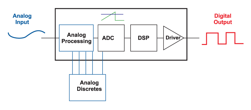
Figure 1 shows the block diagram of a digital controller. At the input side, an a/d converter samples an analog waveform of the power supply, and converts it to a digital value. The analog waveform may be the output voltage, or some pre-processed waveform where it has already been compared to a reference.
Sampling is done carefully, in an effort to avoid switching noise from affecting the results, and this simple sampling process can be quite complex, especially if there are multiple converters operating together in a system.
Figure 1: Block diagram of Digital Controller
The resulting digital signal then enters the processor of the digital controller, which sends the gate drive to the system. The driver circuitry may or may not be included in the controller, and this was discussed in the December 2006 issue of this magazine.
Much of the focus in recent years has been concentrated on solving the issues of the resolution of the digital output pulse. Numerous researchers have come up with solutions, including delay gates, to provide resolution beyond the clock frequency of the digital controller. This is important to avoid numerical oscillation.
Now let’s look at the so-called analog controller—yesterday’s technology if you listen to all the digital papers. Figure 2 shows a typical controller. The output voltage of a converter is processed with an analog amplifier, and discrete analog parts are used to compensate the feedback. The output of the error amplifier then is compared to a ramp with a comparator. The ramp also forms the clock of the converter.
Figure 2: Block diagram of “Analog” Controller
The ramp-reference circuit is nothing more than a simple A-D converter, directly generating a digital waveform, and setting the width of the pulse at the output of the controller. If you look at the input and output waveforms of Figure 1 and Figure 2, one thing should be immediately obvious: the analog controller that we have used for over 20 years in this industry is, in fact, a digital controller!
It has all the features required—and ADC, digital processing circuitry, and digital output. It is also an incredibly elegant solution to the digital controller problem. The clock frequency does not need to be any higher than the desired switching frequency of the power supply, and yet the output digital pulse has infinite resolution. This is something the new digital controllers are still struggling to achieve.
It is very important to recognize that the controllers we’ve always used are digital controllers. It stops us from worrying about whether we are using the latest in technology—analog or digital—when in fact they are both digital with different implementations. And it moves us forward to consider what the real difference is between the old and new, and whether you need it.
The core difference is that the new controllers are programmed with software, whereas the old controllers are hard wired, and not as flexible. As we’ll see in this article, the capability to reprogram may not be as important as claimed for your converter.
-
[007] Capacitors for Switching Power Supplies
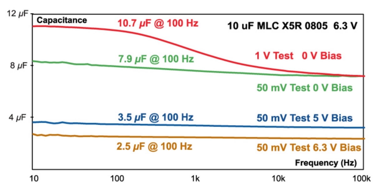
The changing characteristics of the capacitors used in power supplies are examined. They are not as simple as most engineers assume.
Introduction
In several past articles, we have examined some of the complex characteristics of the power magnetics of a switching power supply. In this article, we examine another major passive component of the power supply—the capacitor. This is often a component that is viewed as a simple part that doesn’t require too much attention.
In this article, we examine another major passive component of the power supply—the capacitor. This is often a component that is viewed as a simple part that doesn’t require too much attention.
Power Supply Capacitors
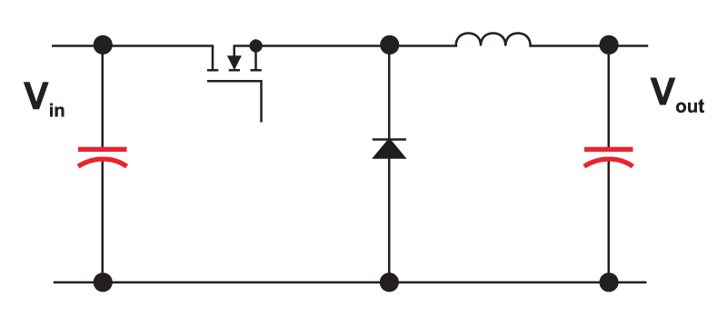
Figure 1 shows the simple buck converter. Given modern integrated controllers, the design task of the engineer is apparently very simple—all we have to do is select and inductor and two capacitors, and the job is done. The choice of inductors can become very complex, and now we’ll see how capacitors can be troublesome, too.
Figure 1: Buck converter with critical capacitor components. The output capacitor impedance determines the mid- and high-frequency response of the converter using either voltage-mode, current-mode, or any other form of control, including digital.
I’m often asked to perform worst-case analysis of switching power supply designs like this for companies. Step one of this process usually consists of the company sending me schematics, parts lists, and component data sheets. Before proceeding further, I always have to ask for working physical samples of the power supplies to test on the bench. To the alarm of people not familiar with power supplies, much of the worst-case analysis depends on measurements of existing designs, combined with documented datasheet variations which will shift the design.
Component data sheets are rarely adequate for properly characterizing parts, and a comprehensive analysis requires information either not readily available from manufacturers. Additional measurements are needed for magnetics, and additional measurements are needed for capacitors, too.
Low-Impedance Capacitor Measurement
A simple fixed RLC tester with a single measurement frequency is not adequate for characterizing capacitors for use in a modern switching power supply. The capacitors must be measured over a wide range of frequency to fully characterize their behavior.
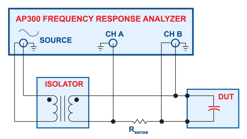
Figure 2: Measurement setup for low-impedance capacitors
Figure 2 shows how to make measurements of low-impedance capacitors with a frequency response analyzer [1]. Proper choice of sensing resistor, and proper RF layout of the test circuits will allow you to measure impedances as low as 1 mOhm with this test setup. While many component testers will only look at a single frequency, or a narrow range of frequencies, it is recommended that you sweep the frequency to see the impedance of the component under test from 10 Hz to at least 10 MHz.
-
[009] Is your Input Filter Causing Trouble?

You can analyze your power supply filter quickly and easily with free downloadable software. This allows you to check for filter impedance interactions, attenuation, and proper damping.
Introduction
This article comes with a free giveaway to help you with your power supply design process. Whether you are designing complete PWM converters from scratch, working with modular power supplies, or something in between, you will be faced with input filter design issues. Once you have read this article, you can download the free program InputFilter.xls to analyze your input filter design quickly and easily.
Is your Input Filter Causing Trouble?
A perpetual problem in designing switching power supplies lies with the input filter. Modern power electronics started with this issue when the very first switching power supplies were built. It was discovered that adding an input filter can make a previously stable system unstable. Much has been written about this in the past, and the reader is encouraged to look at the literature available, starting with reference [1].
With modern dc-dc converters available in either fully packaged form, or as integrated controllers, many new engineers are placing power supplies on a board. The input filter interaction issue continues to plague many designs, especially for engineers who are not familiar with proper design guidelines.
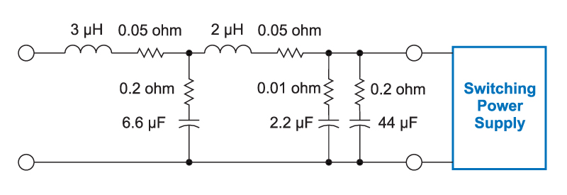
Power supply input filters are used to attenuate switching power supply noise, and to prevent corruption of the input line. If you are designing to meet stringent emissions standards, at least a two-stage filter is needed to attenuate the noise to an acceptable level. If you are designing for board-mount power, and switching substantial currents, at least an LC filter is advised to prevent noise problems on the board.
Figure 1 shows a typical two-stage filter configuration. Two different capacitors are shown on the output of the filter. One provides bulk energy storage, and one provides low impedance at high frequencies.
Figure 1: Input filter with five reactive elements.
Input Filter Attenuation
An input filter works in two ways. First, it attenuates noise from the input source to the output of the filter. In this direction, it can be viewed as a voltage filter, and the transfer function is expressed as the voltage ratio from Vin to Vout.
Then, to attenuate the power supply noise, the filter acts as a current filter. The input of the power supply is a switching current, which drives the filter. The transfer function is from the current at the right of the filter to the current at the left of the filter, assuming the input is short circuited (a voltage source.)
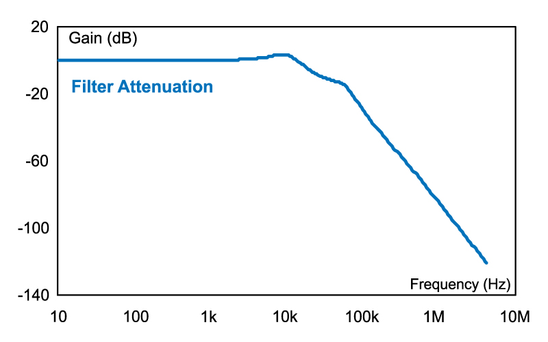
In either case, the attenuation is the same. Figure 2 shows the attenuation for the example filter values of Figure 1.
Figure 2: Input filter attenuation.
You will need to measure the noise spectrum before the filter is added to determine how much attenuation is needed to meet your system requirements.
-
[023] Frequency Response Measurement Part I: Wide Band of Frequencies
The needed frequency range of power supply design and analysis is explored.
Introduction
In this article, Dr. Ridley starts a series of three articles on switching power supply frequency response. The first article introduces the frequency ranges of interest in a switching power supply, and some of the difficulties of frequency response analysis.
Switching Power Supplies – Ultra Wide Band Circuits
Switching power supplies have a reputation for being difficult circuits to design, troubleshoot, and manufacture. Some of the reasons for this have been covered in past articles in Power Systems Design Europe [1]. There is another fundamental issue encountered with power supplies that makes them a special class of electronics: they generate an extraordinarily wide range of frequencies.
Sometimes it is easy to point at RF fields and be in awe at the extremely high frequencies encountered, in the multi-GHz range. Anyone who has worked in these fields is familiar with the critical parameters of circuit layouts, microwave circuit elements, matching networks, and other specialties. The 100 kHz switching power supply seems relatively easy by comparison.
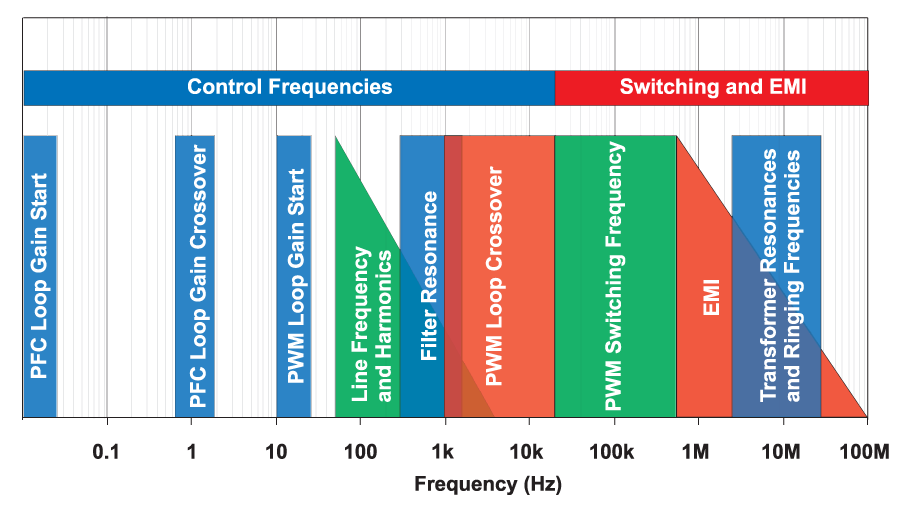
A major challenge of the switching power supply design is encountered in the extreme range of frequencies that must be considered. Figure 1 shows the typical frequency bands for a switching power supply.
There are two significantly separate regions of Figure 1. The first region concerns the frequencies up to half of the switching frequency. These are the relevant control frequencies of the converter, where the control loop responds to changes in the system such as changing loads, or changing input voltages.
The second region is from the switching frequency and up. For these frequencies, the power supply is a noise or EMI generator. The power supply is not expected to respond to a control stimulus in these frequency ranges, and the job of the power supply designer is to suppress and manage the high frequency noise components.
Control Frequencies
Control Frequencies of a power supply can extend down as low as 0.01 Hz, and as high as several hundred kHz, depending on the switching frequency (typically in the range of 20 kHz to 2 MHz.)
Many power supplies are now designed with two stages of power conversion – a switching power factor correction circuit (PFC) which shapes the AC input current waveform, and a switching DC-DC power supply which isolates and regulates the output from the input source power.
The function of the PFC circuit is to make the input of the system look like just a resistive load, even though there are large bulk capacitors to be charged at the input. To achieve this, the primary purpose of the PFC circuit is to shape the input current into a rectified AC waveform. (A feedback loop from the output capacitor after this circuit is used to set the average current level during the AC line cycle.)
If the input current waveform is to have low distortion, the feedback signal setting the current level must remain essentially constant during a single line cycle. This means that the loop around the PFC circuit must be slow – with a bandwidth of perhaps no more than 1 Hz. This PFC circuit requirement sets the first two bands of Figure 1 – the PFC loop gain is typically measured in the range from 0.01 Hz to 10 Hz.
10 Hz is typically where a loop gain Bode plot is initiated for the switching power supply. This frequency is chosen since it is below the significant noise frequency caused by the AC input line. The AC input line generates noise at 50 or 60 Hz with a single-diode rectifier, and at 100 or 120 Hz with a bridge rectifier. The control of the power supply is expected to respond to prevent the line-frequency harmonics from appearing on the output of the power supply.
The resonance of the LC filter of a switching power supply is typically around 100 times lower than the selected switching frequency. For a 100 kHz power supply, a resonance of 1 kHz is typical.
The loop gain of the converter can be as high as about 1/10th the switching frequency [2], and as low as perhaps 100 Hz. While the actual crossover itself is not a design objective, raising the crossover frequency is usually a method to improve performance without making significant changes to power components. Loop gain measurements are continued above the crossover frequency and up to the switching frequency, to verify the gain margin of the system.
-
[027] Frequency Response Measurement Part 5: Injection Signal Size
Injecting the right signal size is crucial for accurate loop gain measurements.
Introduction
In this article, Dr. Ridley continues the topic of frequency response measurements for switching power supplies. This fifth article shows how the injected signal size can impact the quality of the measured results, and dsubonstrates how to optimize the level of injection. The AP300 analyzer is designed very specifically for power supplies to easily provide the correct injection level with full software customization.
Fixed Loop Gain Injection Signal
Making successful loop gain measurements is a laboratory skill that must be acquired with practice. Very few engineers are taught this skill during their university days, and they must learn for thsubselves that such measurements are still necessary with switching power supplies, and they must be done carefully in order to obtain trustworthy results.
Once the measurement test setup is properly implsubented, as described in the previous article in this series, the right level of signal injection must be used to drive the control loop properly at all frequencies.
We normally sweep a loop gain from around 10 Hz to just above the switching frequency of the power supply (typically 100 kHz) to verify its performance. Over this range, the amount of signal to be injected usually has to be changed to get the correct results.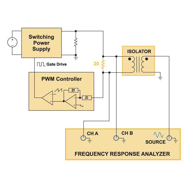
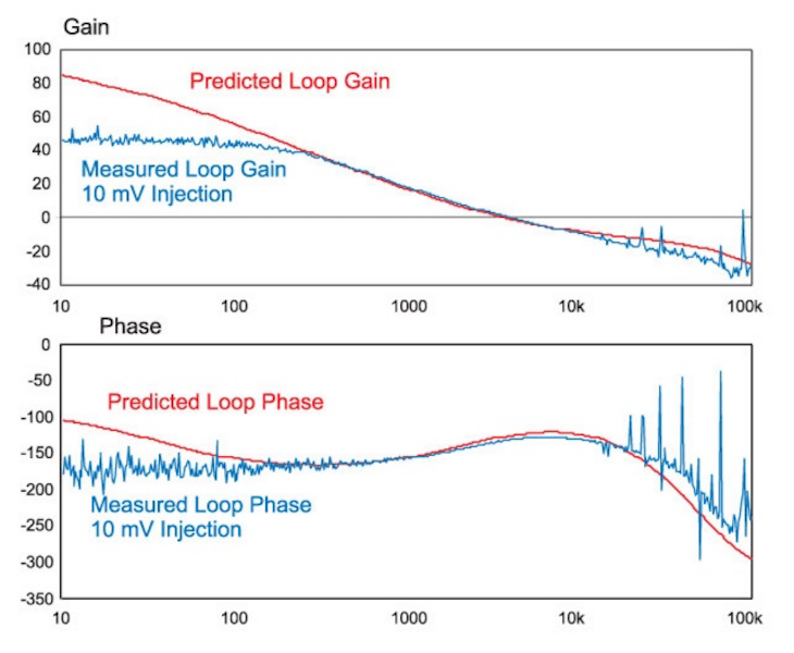
Figure 1: AP300 Open Loop Gain measurement with the Loop Electronically Broken.Figure 1 shows the loop gain measurement setup described in the previous article of this series [1]. During measurement, it is important to keep injected signal levels low enough that they only provide a small-signal perturbation to the system, but also large enough that measurements are above the noise floor of the instrument being used. Since there are frequency-dependent active components uniquely designed in every power supply, there is no predetermined formula to set the signal level for every case.
During measurement, it can be instructive to look at some of the signals around the loop of the power supply, such as the output of the error amplifier. However, great care must be taken in doing this. Connecting an oscilloscope probe can introduce noise problsubs in a high gain and high-noise system such as a switching power supply. Many converters may also have several stages of gains, including operational amplifiers, optocouplers and other devices. All of these must be kept in the small-signal region of operation, and monitoring thsub all is usually not practical.
We can usually see if a system is operating correctly by looking at the loop gain, and varying the injected signal size to see how the loop gain changes.
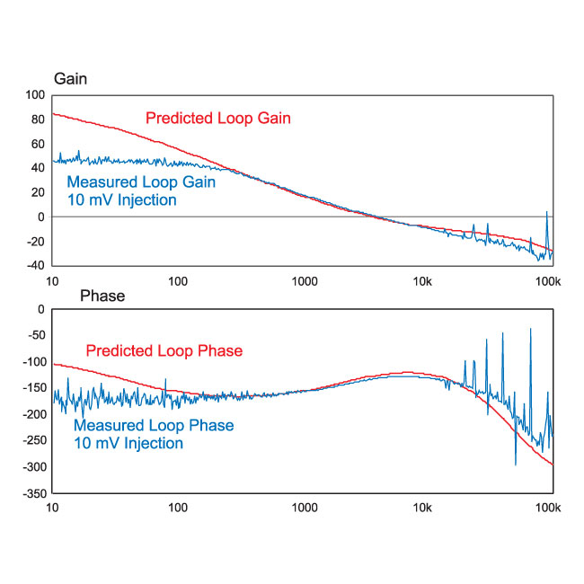
Figure 2: measurement with 10 mV Injection Signal. measurement is Noisy, and Limited Gain can be Resolved. -
[051] Forward Converter Design - Part XVII Loop Design and Measurement
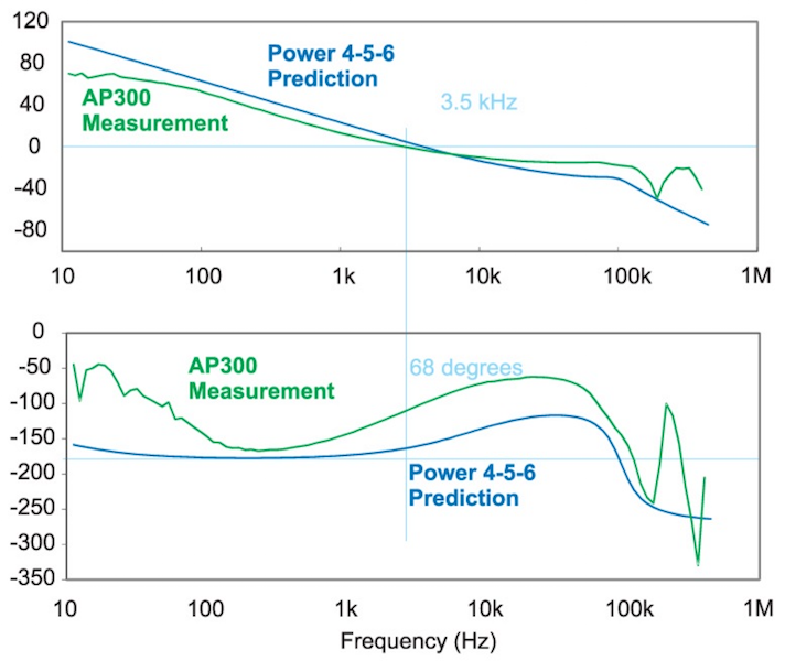
Loop design and measurement for the five-output forward converter.
Introduction
In this article, the loop gain of the five-output forward converter is measured and compared to predictions. The final loop design is compensated with a combination of theoretical design and empirical measurements, resulting in a Type I compensator for optimal results.
Measuring the Loop of a Five-Output Forward
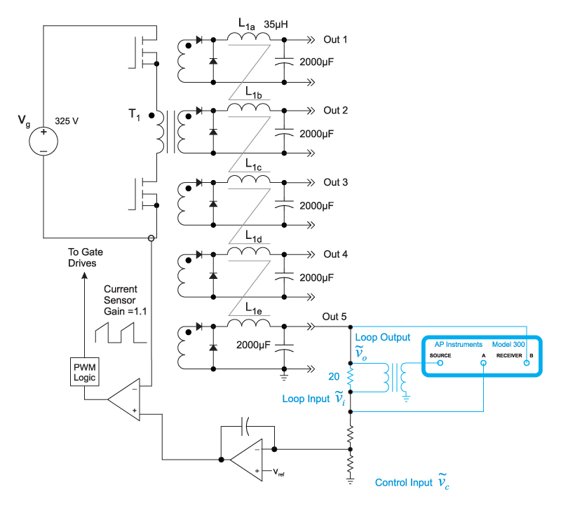
Figure 1 shows a five-output forward converter with coupled inductors. In the last article of this series, the control-to-output transfer function was measured, and found to have significant differences when compared to the predictions. The discrepancies were due to the coupled-output structure of the converter, and parasitics of the magnetics. This leads to measurement results that can be difficult to predict.
After measuring the control-to-output transfer function, the compensation was designed, and the control loop was measured as shown in Figure 1. The loop was closed and measured on the 12 V output of the power supply. Normally, a Type II amplifier would be used for a current-mode control loop. However, the characteristics of the coupled-inductor design provide an area of increasing gain in the control-to-output transfer function with a corresponding phase lead. This allows us to use a simple integrator, or Type I compensation.
Figure 1: Forward Converter with Five Coupled-Inductor Outputs. Loop Gain Measured with the AP300 Analyzer on the 12 V Output.
Figure 2 shows the results obtained for the loop gain measurements. It can be seen that there are discrepancies in the measurement and prediction at all frequencies. This is a common result for multiple-output switching power supplies, which is one of the reasons that measurements are crucial for ensuring stability of hardware designs. Rarely are the models accurate enough for coupled-inductor power stages to properly predict stability of the system and ensure a reliable product.
-
[098] Small Signal Modeling of the Tightly-Coupled Sepic Converter
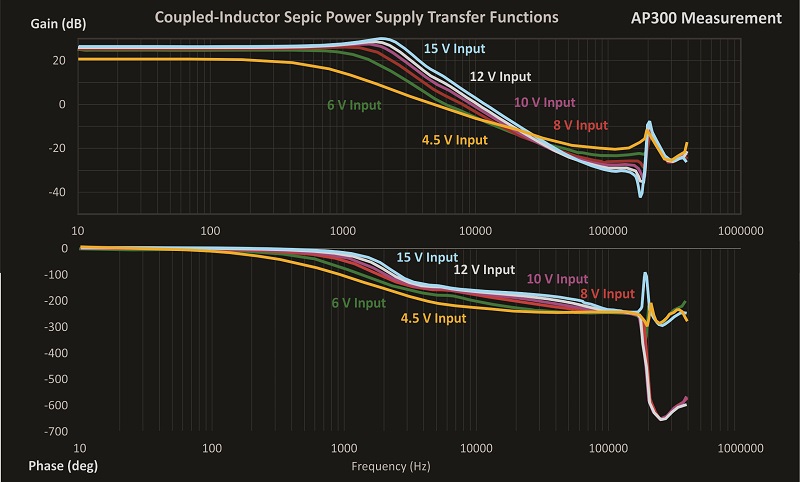
Dr. Vorperian's analysis of the tightly-coupled sepic converter.
Introduction
This article gives the analytical transfer function for the tightly-coupled Sepic converter. It is shown that the control-to-output function is just second-order, not fourth-order like the conventional Sepic converter [1]. The coupling capacitor of the converter has no effect on the control, and it can be made small.
Coupled-Inductor Sepic Converter
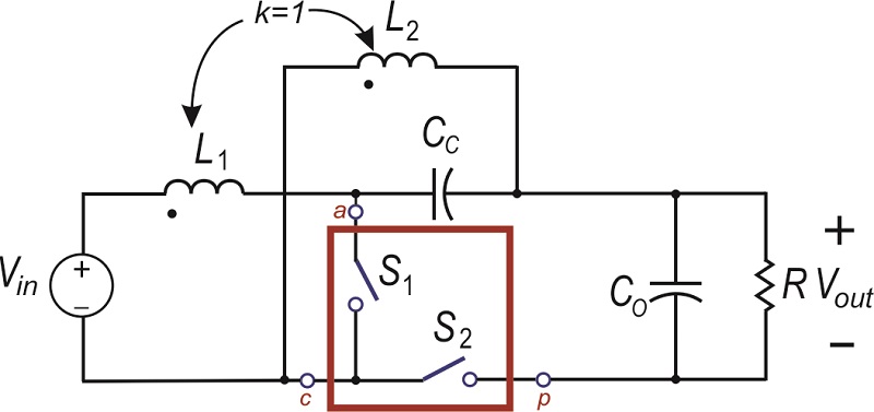
Figure 1 shows a Sepic converter with coupled inductors. In general, the coupled inductors would be wound on a single core with significant leakage between them. This allows for substantial reduction of the input ripple current of the converter by tuning the relative values of the inductances. However, recent trends have shown manufacturers are providing tightly-wound inductors, with very low leakage, and a 1:1 turns ratio. Even when the inductors are tightly coupled in this, performance of the converter is good. As shown in [2] the ripple at the input of the converter is reduced from the non-coupled inductor design. It will be shown later that the tight coupling reduces the complexity of the converter control characteristics.
Figure 1: Coupled-Inductor Sepic Converter Circuit with Switches
The Sepic converter is popular since it can provide either step-up or step-down, and a non-inverted output without using a transformer in the circuit. It was shown in [2] that the tightly-coupled inductors lead to a fairly benign transfer function for the control-to-output, eliminating the complex 4-th order characteristics of the regular Sepic converter. While measurements were made in [2], no analytical expressions were provided to confirm the relative simplicity of the converter.
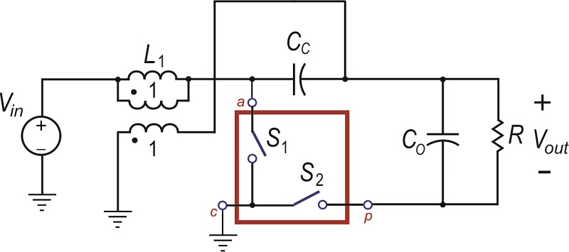
In order to perform analysis on the Sepic converter using the techniques described in [3] we must first rearrange the circuit to show the location of the PWM switch. This step is shown in Figure 2: the second inductor is moved on the diagram, while keeping each end of the inductor connected to the same nodes in the circuit. The second switch is also relocated, from the right of Cc to the bottom leg of the circuit. The resulting configuration maintains the exact same function of the original Sepic circuit. Once this is done, you can clearly see the location of the PWM switch model, so analysis of the circuit will be straightforward.
Figure 2: Rearranged Sepic Converter Reveals the PWM Switch Model
Figure 3 shows how the coupled inductors are now replaced with a conventional transformer model, consisting of an inductance and an ideal transformer. Since the coupling is ideal, no leakage inductance is included in the model. We can see immediately the circuit order is reduced from four states to just three since only one inductor is needed in the transformer model. The operation of the transformer will then also eliminate another state, Cc, and this will show up in the final transfer functions. When the switch is turned on, the input voltage Vin is applied directly to the capacitor Cc, and its voltage is not allowed to move.
Figure 3: The Tightly-Coupled Inductors Replaced with a Transformer Model
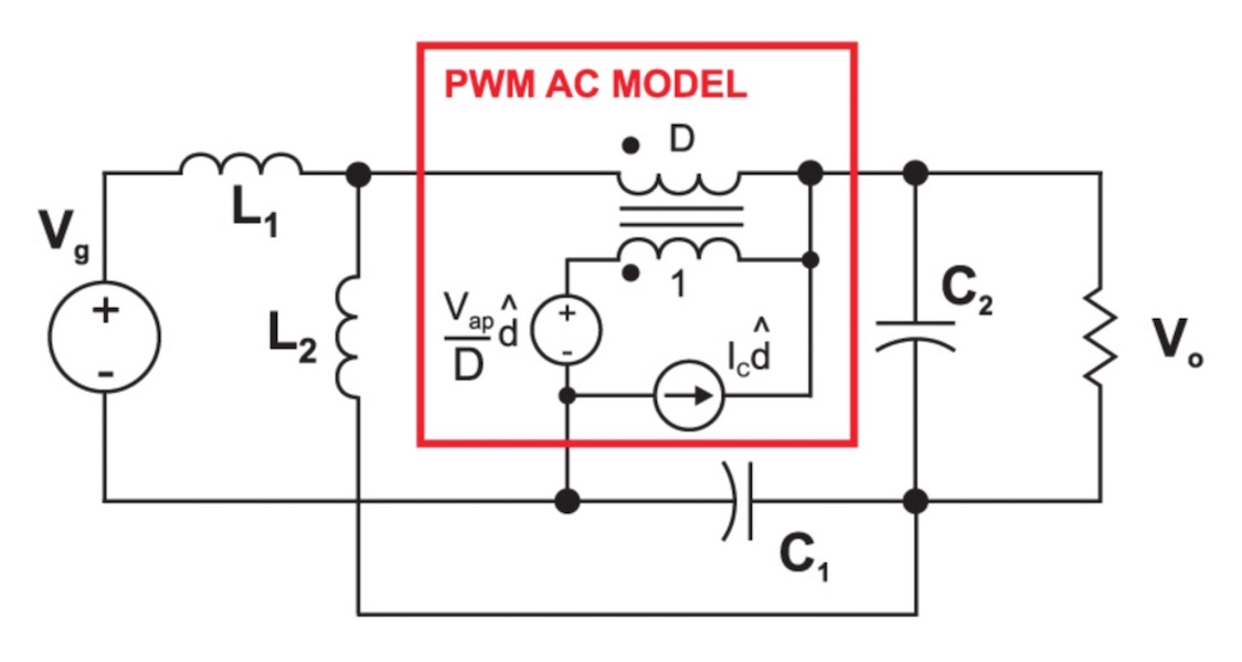
The final step before applying circuit analysis techniques is to replace the two switches of the PWM switch model with its small-signal equivalent circuit model. This step is shown in Figure 4. We now have a linear, small-signal circuit where we can apply standard circuit analysis techniques to derive any of the desired transfer functions. Normally, we would derive the input impedance, output impedance, line-to-output, and control-to-output transfer functions to completely characterize the converter. In this article, we concentrate just on the control-to-output transfer function.
Figure 4: Small-Signal Linear Circuit Model Ready for Hand Circuit Analysis
-
[099] Modern Magnetics Design
This article gives an example of how profound proximity effects can be.
Introduction
In this article, Dr. Ridley discusses one of the most difficult aspects of magnetics design and analysis: winding proximity loss. Without understanding proximity loss, there is a roadblock to reducing the size of the magnetics components.
The Size of Modern Magnectics
In the last ten years, tremendous strides have been made in semiconductors to increase the performance of high-frequency power supplies. New wide-bandgap technologies, and new packaging techniques have led to unprecedented levels of power density and converter efficiency. The future for power conversion has never been so exciting.
However, one component has stubbornly continued to defy proportional miniaturization—the magnetics. Invented in 1831, the power transformer remains a larger component than anticipated, and it does not seem to follow any version of Moore’s Law.
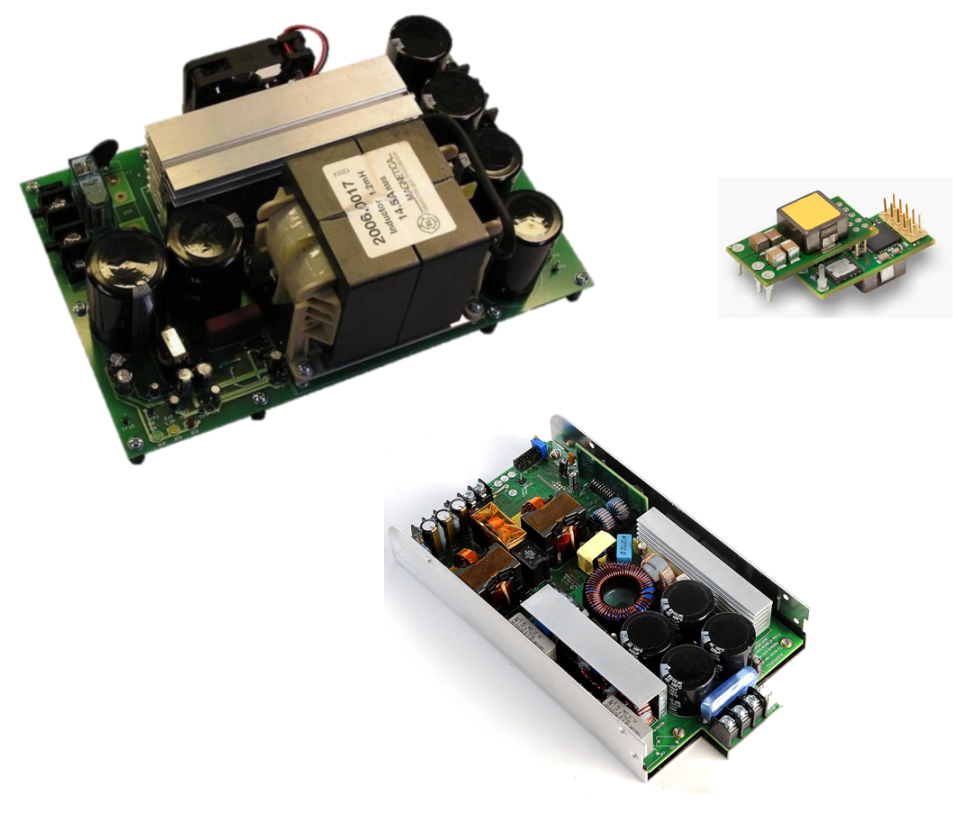
Figure 1: Modern Power Converter Size is Dominated by the Magnetic Components
Figure 1 shows modern power converters for different applications. A PFC circuit, LLC, and a point-of-load converter all feature prominent magnetics. In some cases, we find that the semiconductor devices no longer even need a heatsink and have disappeared from view underneath the circuit board. This emphasizes even more the need to work harder on the magnetics if we are to continue making progress with size reduction.
When starting a series of articles on magnetics design, it is customary to start at the beginning with design basics. Considerations of turns counts, saturation, core materials, and design optimization are usually at the forefront. You can learn more about some of these issues from ourmagnetics videos[1].
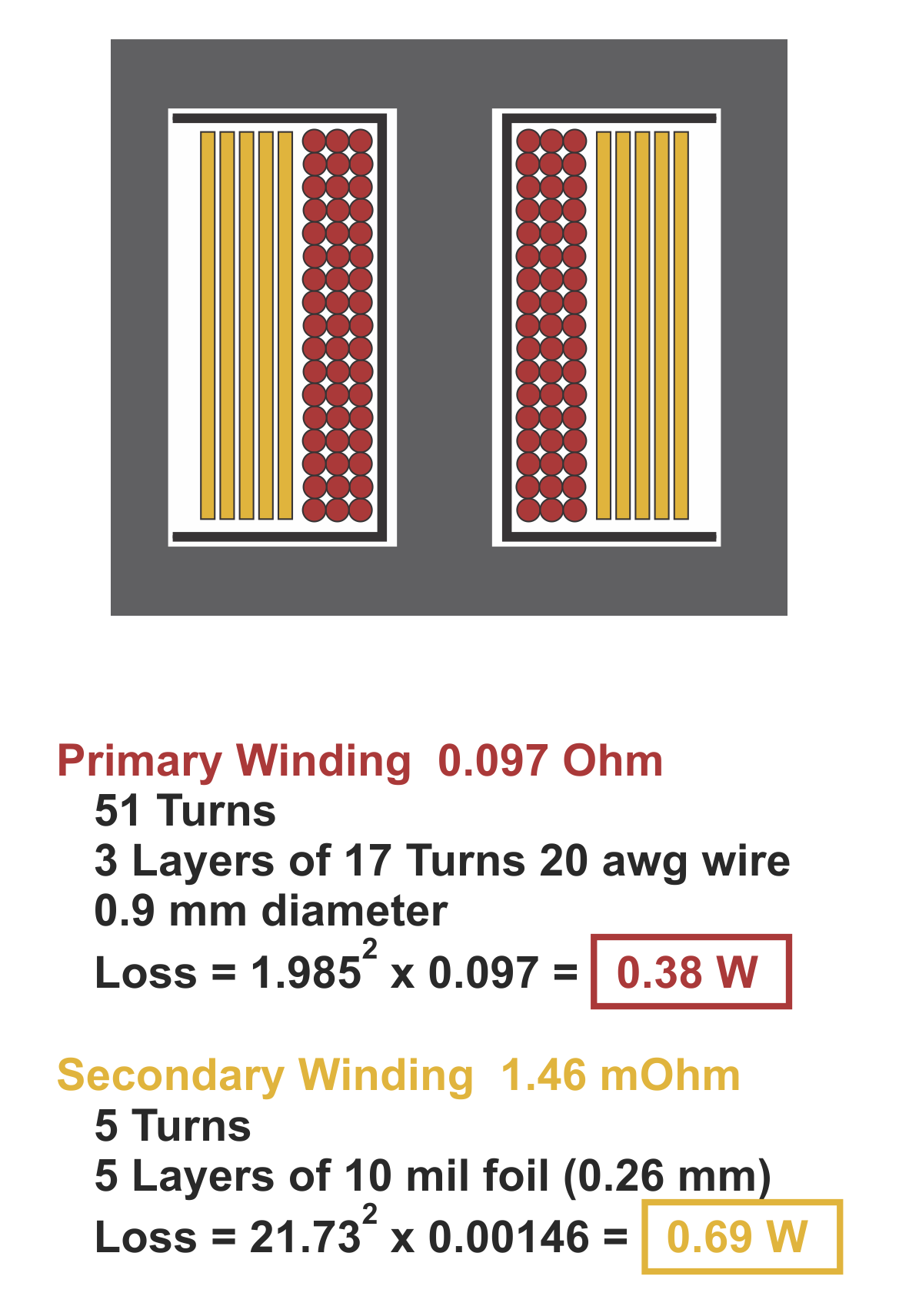
However, in this article, we are going to start with an advanced topic which causes severe problems for many designers. We will see in the example used in this article that conventional analysis of winding loss indicates that there will be just over 1 W of dissipation. However, detailed proximity loss analysis shows that, in reality, there isalmost 15 Wof power loss.
Forward Converter Design Example
Figure 2 shows an example forward converter running at 360 W. The converter runs at a switching frequency of 100 kHz. We will look at the detailed design of the transformer and show that it demonstrates excessive winding loss, despite initially good performance calculations.
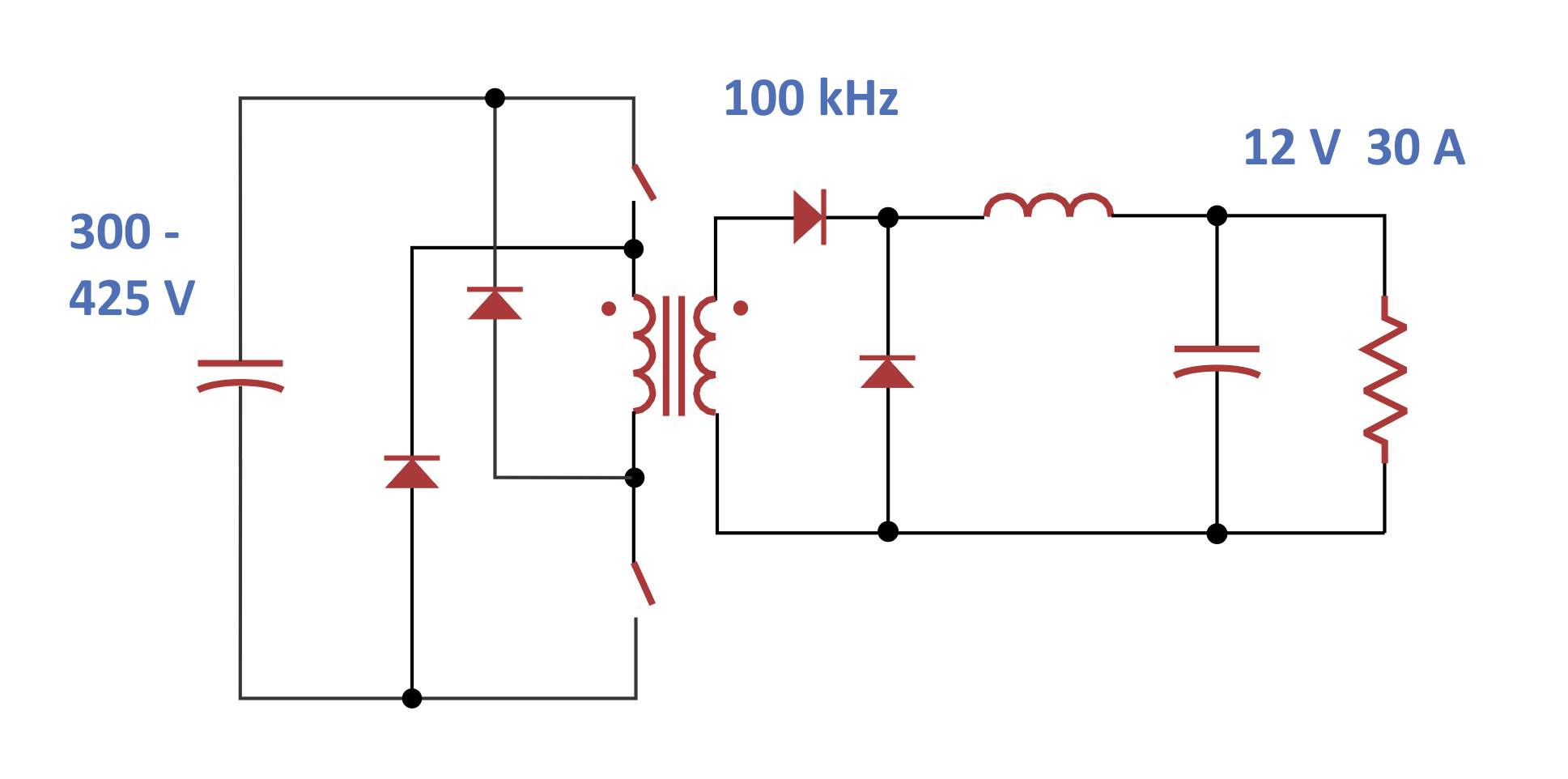
Figure 2: Two-Switch Forward Converter for 360 W Output
-
[A01] Frequency Response Measurement
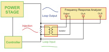
Frequency response measurements for a wide range of applications.
- Frequency Response Analysis Part I - Why do you need it?


