


Flyback design specifications and architecture.
Introduction
This article is the first of a series in which Dr. Ridley shows the steps involved in designing and building an offline flyback converter. The first part of the series presents the power supply architecture and schematic, including the control and bias circuits.
Flyback Power Converter
The offline flyback converter is a topology that is found in many applications. It serves as a bias supply for other power converter topologies, or as the main supply for low-power electronics systems, typically 50 W or less. The flyback is usually selected for the following reasons:
- Low parts count
- Single magnetic element
- Single ground-referenced switch
- Ease of generation of multiple outputs
The disadvantages of the flyback converter are pulsating input and output currents, and a voltage stress on the switch that exceeds the input voltage. At low power levels, these issues are less important than the flyback advantages.
Power Supply Requirements
The specifications for the power supply were as follows:
- Input Voltage: 185 – 265 AC
- Output 1: 15 VDC @ 1.4A isolated +/-10%
- Output 2: 15 VDC @ 50 mA nonisolated (bias and regulation supply)
- Maximum power: 22 W
- Power Topology: Flyback
- Controller: 384x Controller from Texas Instruments
The main output provides a relatively constant current, and the regulation range of 10% should be achievable through cross-regulation to the bias winding supply.
Block Diagram and Circuit Schematic
Figure 1 shows the block diagram of the flyback power converter with the control, bias, and power stage blocks. Both the power stage and the bias circuit are fed directly from the rectified ac input line.
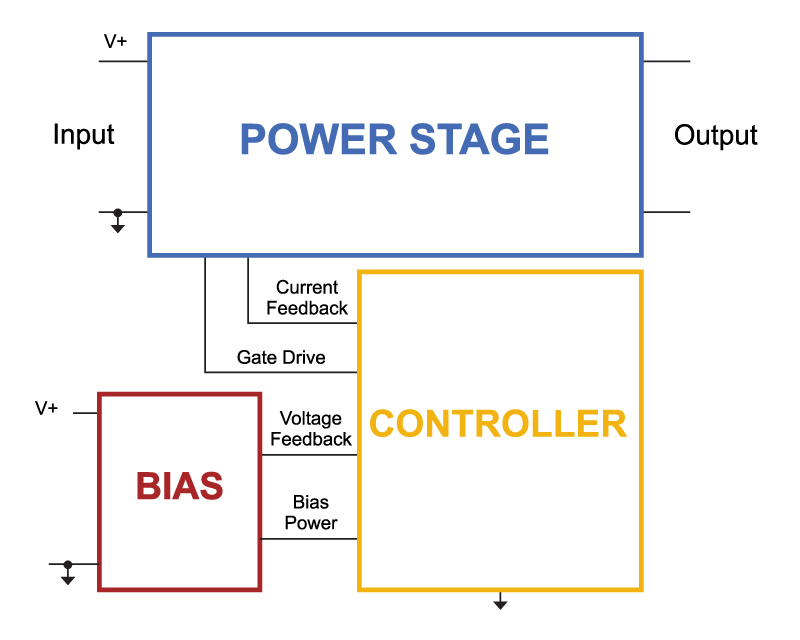
Figure 1: Three parts of a flyback converter – bias, control, and power stage with interconnect signals
The function of the bias supply is to provide the operating voltage to the control circuit, and to do this with minimal dissipation.
The controller sends a gate drive signal to the power stage, and receives a current-sense signal from the power stage, used to protect and regulate the converter. Voltage feedback for the control loop is derived from the bias circuit, so there is no need for isolated feedback from the power stage. The choice of the correct controller from the UC384x family of parts will be discussed in a later part of this series.
Figure 2 shows the complete schematic of the flyback power supply system. In this series of articles, each of the parts of this circuit will be discussed in detail, including test procedures.
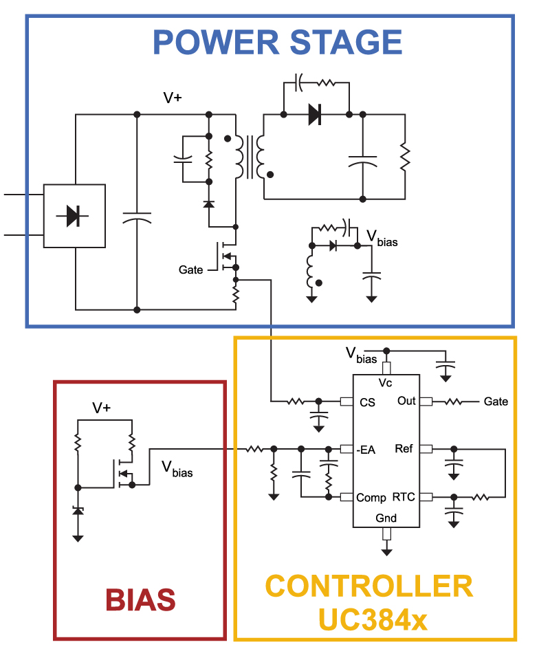
Figure 2: Schematic of an offline flyback converter with control and bias circuits.
Bias Circuit
The bias circuit shown in Figure 2 consists of just a few parts. A FET is used as a linear regulator to start the control chip and its gate is fed by a resistor and zener diode combination. A secondary winding is added to the power transformer to provide the bias power once the main circuit reaches regulation, and the linear regulator is then automatically shut off. This simple circuit provides a rugged and efficient way to power the controller.
Control Circuit
The 384x series of current-mode controllers were selected since they are readily available from multiple sources and are low cost with high performance [2]. While this family of controllers may seem outdated, they are still used extensively by experienced power designers and power supply companies who wish to have full control over all of the waveforms of the circuit. This will be discussed in detail later in this series of articles.
Power Stage
The power stage shown in Figure 2 includes a power FET with voltage clamp, current sensor, transformer, output diode with snubber, and output capacitor. A second output winding on the transformer, together with another diode and capacitor, feeds the bias circuit voltage. Having a discrete FET design allows much greater design flexibility than working with integrated controllers where the power FET is on the same die as the control circuitry. Also, higher voltage parts are available in the discrete FET package, and this can be important for rugged design.
PCB Layout Design
This may not be welcome news to those who are about to embark on their first power supply design, but the first thing that needs to be done is a board layout. It is not a good use of time to try and test controllers and power stage parts with a wired breadboard. There are many critical layout paths in the circuit, and proper placement of parts can only be achieved with a real printed circuit board.
During a power supply development, even a simple flyback, you can count on needing a minimum of two iterations of the PCB. Most projects will iterate the board at least three times by the time it is ready for manufacturing. It is very important to begin your initial testing on the PCB. The board layout creates parasitics and EMI issues that must be resolved as early in the design cycle as possible.
Figure 3 shows a photograph of the double-sided PCB designed for the flyback power supply. Notice that good partitioning of the control, bias, and power stage are maintained on the PCB, and this helps you work on the board later and to achieve good layout.
The details of the layout process are extremely important, and many of the rules and guidelines for proper layout were discussed in some detail in [1]. If you are new to power supply design, the best thing to do is to dive into using a layout program and to learn as quickly as you can by making some boards and testing them. If you are fortunate, you may have someone to mentor you through this process, but most engineers have to learn board layout the hard way, by themselves.
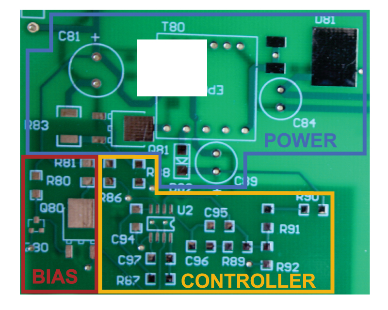
Figure 3: PC board layout of the flyback converter ready for parts population and testing.
Once you become adept at PCB layout, it becomes the fastest way to build test circuits for your power supplies.
Summary
The architecture and schematic of a complete flyback power supply have been presented in the first part of this series of articles. A standard 384x current-mode controller driving a discrete FET is to be used for the power system to provide maximum flexibility of design at a low cost.
In the next article, the input rectifier design and bias circuit will be discussed and test results for this part of the circuit presented.
References
- Join our LinkedIn group titled “Power Supply Design Center”. Noncommercial site with over 7000 helpful members with lots of theoretical and practical experience.
- For power supply hands-on training, please sign up for our workshops.
- www.ti.com/product/uc3842, control chip datasheet.