


Flyback input rectifier and transformer design.
Introduction
This article is the third of a series in which Dr. Ridley shows the steps involved in designing and building an offline flyback converter. The input filter rectifier is simulated to find the design range of the converter, and the transformer design is completed and measured.
Input Voltage Range
The specifications for the power supply were as follows:
- Input Voltage: 185 – 265 AC
- Output 1: 15 VDC @ 1.1 A
- Output 2: 15 VDC @ 50 mA nonisolated (bias and regulation supply)
- Maximum power: 17.25 W (was 22 W)
Notice that between the first article of this series, and this third part, the load on the main output dropped from 1.4 A to 1.1 A. This is common during a power supply development; the end user is rarely finished with design and measurements before the power supply design starts. Being flexible in your design to accommodate changes both up and down in power is just a fact of life for power supply engineers.
The first step in the design process is to determine the actual range of the dc input bus after the rectifier. There is no simple equation to calculate this, and the fastest way to determine the range is to run a simulation, using a constant power load on a capacitor and rectifier. As the design progresses, and input filter and protection circuits are added to the design, the simulation can be modified to accommodate the additional components. Filter inductors, surge resistors and fuses all reduce the actual input voltage to the converter. Trying to incorporate all of this in a calculation is probably not the best use of design time, and simulation is a powerful aid here. Just about any circuit simulator will be able to do this part of the circuit for you, but POWER 4-5-6 was used to generate the waveforms in Figure 1 for maximum speed.
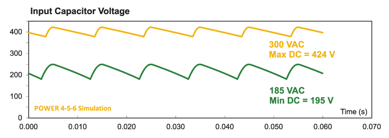
Figure 1: Input line voltage POWER 4-5-6 simulation, showing rectified voltage on a 10 µF input capacitor.
If you were to do true worst-case analysis design, it is necessary to introduce variation in the frequency range of the AC supply, and include the anticipated variations of the input capacitor with initial tolerance and aging effects, but that is beyond the scope of this article.
From this simulation, we see that the maximum voltage seen at the input of the power supply will be 424 V under surge conditions of 300 VAC input. The minimum voltage used to design the power stage is 195 V. For those new to power supply design, this range can be a surprise. Designing for a nominal 240 VAC input results in more than a 2:1 dc input range. This range is obtained using a full-wave input rectifier. If a half-wave rectifier were used, the range would be even larger.
Magnetics Design – Turns Ratio
The first step in designing a flyback transformer is to determine the turns ratio required at low line to give the required output voltage without using an excessive duty cycle. Design approaches vary greatly in choosing the maximum duty cycle. At low power, it is quite common to operate with quite a small maximum duty cycle in order to minimize the stress of the primary power FET. At higher power leverls, some wide-range designs may allow the duty cycle to be in excess of 50% to reduce stresses on the secondary parts and reduce the primary currents.
In this design, the maximum duty cycle was set at 47%. (That is the value that is obtained when selecting a controller than naturally has a maximum nominal value of 50% - a few percent are lost to the finite discharge time of the timing capacitor). With a minimum input voltage of 195 V, a turns ratio of 11:1 provides sufficient voltage to operate the converter over the full specified range with enough margin to control the converter properly.
Magnetics Design – Primary Inductance
While there is a fair amount of leeway in choosing the maximum duty cycle of the controller, and subsequently the turns ratio of the transformer, there is even more freedom of choice in choosing the primary inductor value. Some power designers will select a value to force the converter to operate in discontinuous-conduction mode at all lines and loads. This is the most popular approach for low power flyback designs at 10 W or less.
At higher power levels, this can result in high primary currents, and some designers will select a larger value of inductance to reduce the peak current stresses. The optimal design point is not obvious in most cases, and some experimentation with different designs is beneficial. If you can wind your own magnetics prototypes, this is fast and easy to do, and we teach this process in our design workshops [5].
For this design, the first transformer was chosen to have a primary inductance of 2200 µH. this value runs the converter in CCM at full load, yet it is small enough to make sure the converter is controllable. Figure 2 shows the primary switch current and main secondary diode current that result from this choice of inductor value.
Notice that the peak diode current on the secondary is in excess of 3 A, almost three times the average value of the output current.
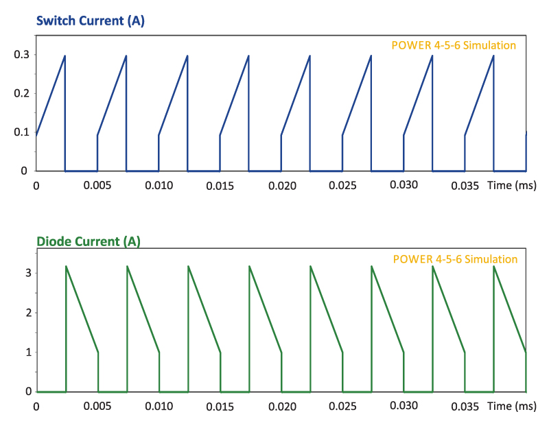
Figure 2: Main FET and diode currents with 2200 µH primary inductance and 11:1 turns ratio.
The primary switch current was just below 0.3 A. The current limiting of the converter was set at 0.334 A, just above the maximum required primary current. Table I shows the calculations used for the transformer design using a TDK EPC19 core. 120 primary turns were needed to support the maximum current at 2200 µH without saturation. 11 turns on the secondary gave the required turns ratio.
| Power | 17.25 W |
| Inductance | 2200 µH |
| Core Type TDK | EPC 19 |
| Core Area | 0.2cm2 |
| Current Limit | 0.33 A |
| Primary Turns | 120 |
| Maximum Flux | 0.305 T |
| Secondary Turns | 11 |
Table 1: Flyback Power Transformer Calculations
The required isolation in the transformer was achieved with the use of kapton-wrapped wire from VIP wire [4]. This gives full triple insulation rating with a minimal thickness of insulation.
The primary was wound in two layers of three segments to minimize winding capacitance and keep the primary impedance as high as possible. More details of this are given in [1]. The winding layout is shown in Fig. 3.
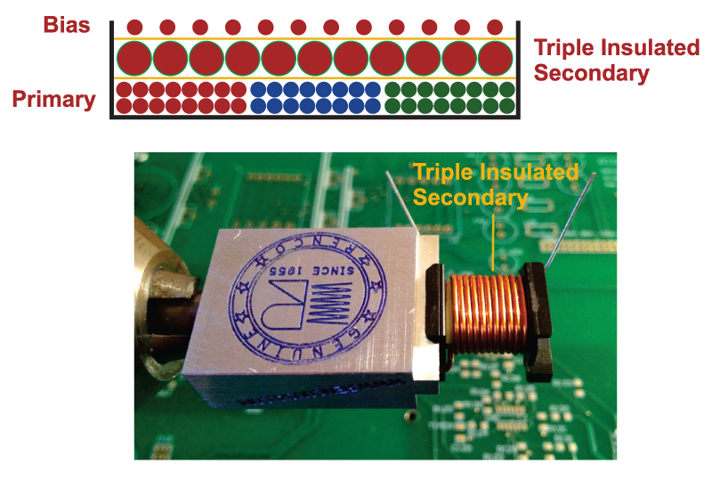
Figure 3: Transformer winding layout. Secondary winding uses triple-insulated VIP kapton wire.
Whenever you build or purchase magnetic components, it is important to do a frequency response characterization before inserting them in the power circuit. This allows you to verify proper design construction, and calculate circuit snubbers quickly from measured transformer parameters. The frequency response is best done on an instrument designed for the job, such as an AP300 frequency response analyzer [2]. It can also be done manually as described in [3].
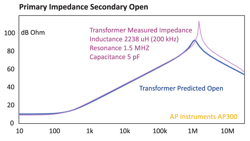
Figure 4: Flyback transformer primary winding impedance with secondaries open.
Figure 4 shows the primary impedance of the flyback transformer measured with the secondaries open. This measurement gives the value of the magnetizing inductance at 2234 µH, calculated at 200 kHz. The resonant frequency was at 1.5 MHz which is produced by an equivalent capacitance of about 5 pF. This capacitance was very low due to the segmented winding structure of the primary.
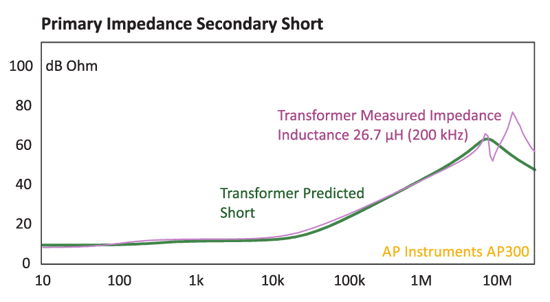
Figure 5: Flyback transformer primary impedance measurement with secondaries short-circuited.
Figure 5 shows the measurement of the transformer primary impedance with the secondaries shorted. The rise in impedance between about 20 kHz and 10 MHz is due to the primary leakage inductance. It can be seen from the curve of the predicted impedance that the slope of the measurement is not quite as steep as 20 dB per decade. This is usually the case for high frequency transformers, and it is caused by proximity effects in the windings. The varying distribution of currents in the winding affects the primary to secondary leakage inductance, and this value is plotted in Figure 6 versus frequency.
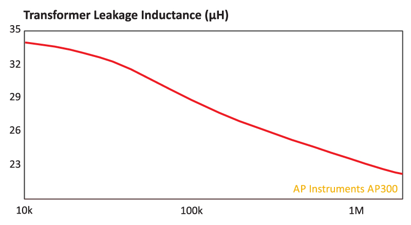
Figure 6 shows that the leakage inductance changes with frequency and it exhibits a significant change from 10 kHz to 1 MHz. It is very important when you specify a custom transformer that the leakage inductance be specified at a given frequency if you want to get repeatable designs and measurements. At 200 kHz, the leakage inductance was measured to be 26.7 µH.
With the transformer qualified, it is ready to be inserted into the power circuit for testing to continue.
Summary
The third part of this series has described the simulation of the input voltage rectifier, main current waveforms, and the construction of the power transformer. Frequency response measurements of the transformer provided the value of the magnetizing inductance, leakage inductance and resonant frequency. With this data complete, the power testing can proceed.
References
- "Flyback Transformer Primary Winding Structures", Ridley Engineering Design Center, Article 53.
- AP300 Frequency Response Analyzer.
- “Manual Frequency Response Measurements”, Ridley Engineering Design Center,
Articles 55-56. - Kapton-wrapped triple-insulated wire, www.vipwire.com