


How inaccurate current limiting can cause problems in low-power flyback designs.
Introduction
For very low power design, around 1 W or less, the DCM flyback converter is a very popular topology. When pushing up to higher power, however, this converter can create difficulties if you do not properly take care of the control parameters—especially current limiting.
Current Limiting and DCM Flyback Design
The discontinuous-mode (DCM) flyback converter is viewed by many designers as being the simplest converter of all. For low power design of several watts, it is often the most prudent choice. The DCM flyback converter works by charging up the primary inductance of a transformer when the power switch is on, and fully discharging the current in the secondary of the transformer when the switch is off. The inductor value, a crucial circuit element, is accurately controlled by gapping the core of the transformer.
The DCM flyback has the following features that lead designers to its selection:
Natural commutation of the output diode, minimizing switching loss and secondary noise;
Low-noise turn-on of the primary switch;
Simple control characteristics; and
Possibility of a quasi-resonant mode of operation to lower noise even further.
The disadvantage of the DCM operation is that the currents in the circuit are higher than for CCM operation.
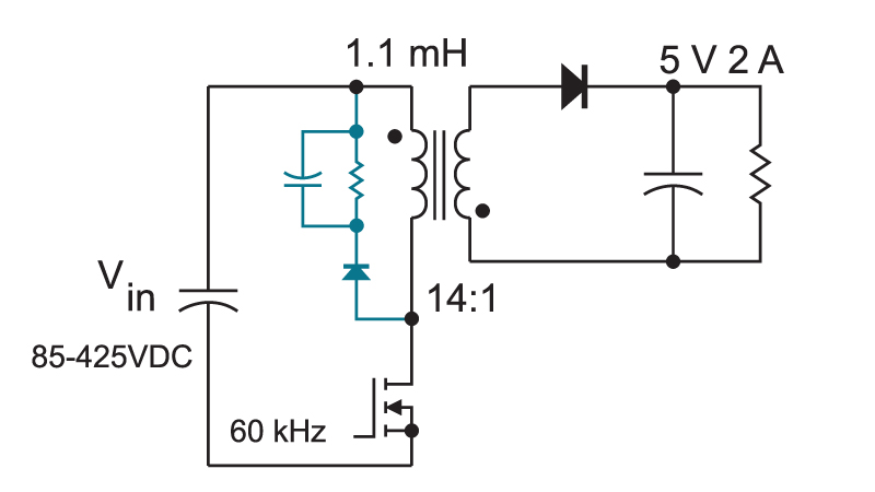
Figure 1: DCM Flyback converter.
In the field of power electronics, there is always a tendency towards higher power. System designers see the features they could add to new products, and inevitably increase the power requirements. Similarly, in applications like appliances, the role of power electronics is on the increase, and older mechanical parts are being replaced by electronics parts that need more power.
The same designers who worked on the low power applications are pushing to 5 W, 10W, and beyond. They are taking with them their design experience at low power, and are encouraged by silicon chip makers who are pushing the capabilities of their integrated switchers to higher and higher power levels.
This is getting a lot of designers into trouble. Design practices that they could get away with at 1 W are not so forgiving of rigorous testing at higher power levels.
DCM Design Constraint at Low Line
Along with increasing power requirements, there are very wide input ranges available for design. It is common for a power supply to need to operate from 85 to 265 VAC continuously, and even wider than that for high-reliability power supplies. With input ripple considerations, and surge requirements, the input line can range from about 85 to 425 VDC. DCM operation must be maintained under all conditions according to many design engineers, even at low line condition.
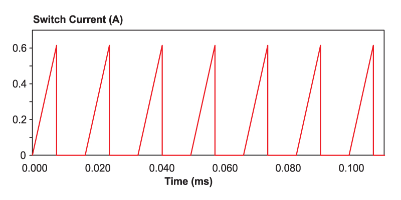
Figure 2: Power switch drain current at low line, full load.
Let’s suppose we have a 60 kHz converter, with a 10 W output. Figure 2 shows the current in the power switch at low line. Typically, when using controllers with integrated power switches, most designers will restrict operation to 50% duty cycle in order to limit the peak voltage on the power switch.
For this converter, the choice of inductor to make the converter operate in DCM is 1.1 mH. The peak current, shown in Figure 2, is 0.61 A.
Choosing a Controller
Now let’s suppose you want to choose an integrated converter controller for this application. ST Microelectronics [1] provides a popular series of parts with their VIper chips.
Possible choices from ST Microelectronics are:
VIper 22
This chip has a current limit of 0.7 A, and has a recommended power of 12 W for wide range input. However, this current limit has a tolerance of +/-20%, so the converter cannot work with this. It also has an on-resistance of 31 ohms at high temperature, which is too high for low-line operation.
The VIper 32
has a current limit of 1.45 A, again with a 20% tolerance. This seems to be the most logical choice with an on-resistance of 11 ohms at high temperature. For the operating conditions of figure 2, this causes a conduction loss of 0.62 W.
The VIper 53 is
designed for considerably higher power with a current limit of 2 A.
Overload Testing
There are many conditions which must be tested on your power supply design. High-line, low-line, light load and full load are just the beginning. Another test which is recommended is short-circuit testing, as described in [2].
The short circuit test is severe, and thoroughly tests the capability of the controller to shut down quickly without the current running out of control.
Another test that must be done is overload testing. The load on each output of the power supply should be increased gradually until the converter starts entering current limit. With the DCM flyback converter, overload testing can produce some surprises.
For the converter described so far, the normal peak current is set at 0.61 A. The DCM flyback operates by sending pulses of energy from the primary to the secondary and the resulting total energy transfer is given by ½ LIp2f.
For the control chip chosen, the worst-case peak current is 1.8 A. This is three times the normal peak current, which leads to nine times the power capability for the converter if it stays in DCM all the time!
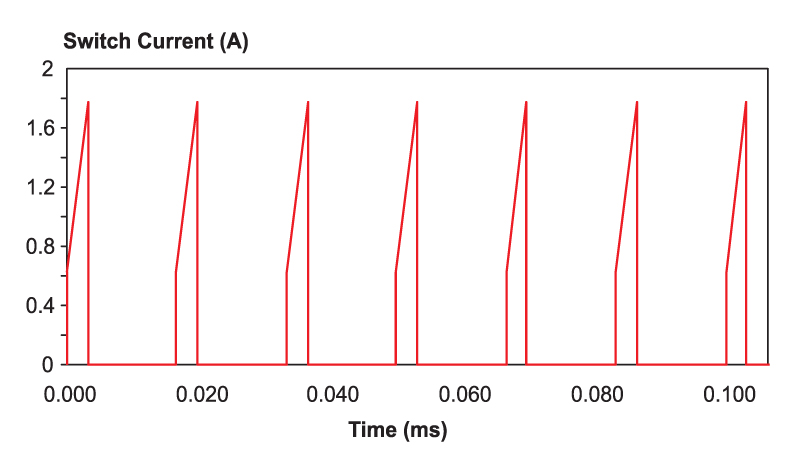
Figure 3: Power switch drain current with seven times the rated load at nominal operating frequency.
Figure 3 shows the overload current in the power switch with 7 times the rated load. A power supply which was designed for 10 W operation must now be able to operate around 100 W (taking into account variations in frequency and inductor tolerance) without any safety issues. Clearly, this presents a significant challenge to the designer in making a safe converter. Magnetics must be grossly over-designed for safe thermal parameters and non-saturation of the transformer.
Notice that the waveform of Figure 3 shows that converter is now in continuous conduction mode, shown by the initial step in the current when the switch turns on. This causes current limit to activate at just 7 times rated current instead of 9 times. In general, operating in CCM reduces sensitivity to inaccurate current limiting. However, it does result in a different transformer design.
The large overhead in current limiting also produces considerable stress on the converter during start up and other transient conditions. The tighter the current limit can be kept, the more reliable the converter will be.
Summary
As power levels rise above 2-3 W, the choice of the DCM flyback converter for the power topology must be given careful thought. If it is to be used with integrated controllers, the most difficult aspect of the design procedure is incorporating proper current limiting. If you are running into problems with high power testing, design options include:
Select a topology that can run in CCM and DCM
Use a controller properly matched with the right current limit for your design
Change to a discrete controller and FET for higher power applications so you can set precise current limits by choosing your own current sense resistor.
Do not overlook the fact that you should be doing overcurrent testing, in addition to short-circuit testing. Short-circuit testing is actually quite benign in terms of thermal stress placed upon your design.
Power supply designers that work in the kW power range often add the additional expense of very precise current limiting, within 1 or 2 percent of the rated load. Lessons should be taken from the high power designs and applied to the low power field.
Additional Reading
- Join our LinkedIn group titled “Power Supply Design Center”. Noncommercial site with over 7000 helpful members with lots of theoretical and practical experience.
- For power supply hands-on training, please sign up for our workshops.
- ST Microelectronics website, www.stmicro.com
- Power Supply Stress Testing