


The "simple" flyback converter exhibits very complex ringing waveforms due to circuit parasitics.
Introduction
PWM power supplies are plagued with ringing waveforms that can degrade performance, impact EMI measurements, and even cause failure. This article explores some of these ringing waveforms, and gives a laboratory technique to measure them easily and safely.
Simple Flyback Converter
The flyback converter is widely used in industry, but many designs do not provide the needed the safety margins needed for modern products. A major cause of this is the ringing waveforms that exist in the converters.
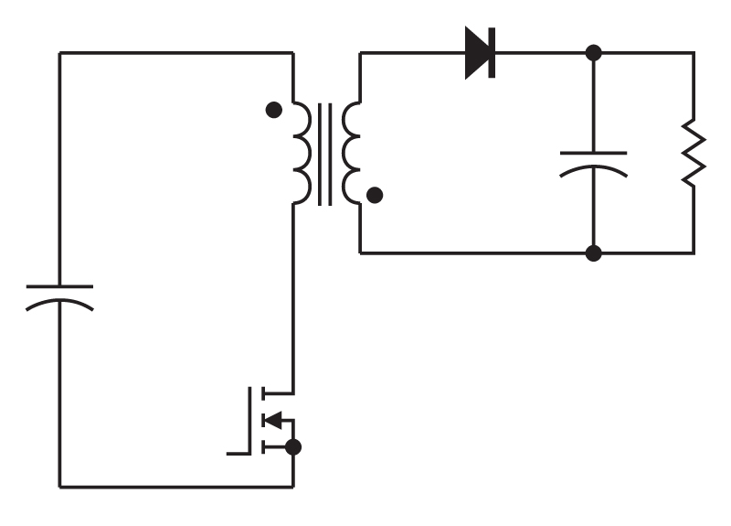
Figure 1: Simple flyback converter with main power stage components
Figure 1 shows a basic flyback converter. Ideally, this converter has square-wave waveforms across the power semiconductors. In reality, there are numerous parasitic elements that cause ringing in the circuit when the semiconductors are turned off.
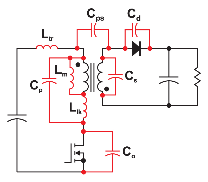
Figure 2: Flyback converter including major parasitic components, shown in red.
Figure 2 shows the dominant converter parasitics. These include:
Board trace inductance Ltr Transformer leakage inductance Llk Transformer magnetizing inductance Lm Transformer primary capacitance Cp Transformer primary-to-secondary capacitance Cps Transformer secondary capacitance Cs FET output capacitance Co Diode junction capacitance Cd
This complicated circuit is actually a simplification of the real circuit. The capacitances shown are bulk capacitances which are actually made up of many distributed capacitances. Furthermore, elements can be voltage dependent, in the case of the semiconductor junction capacitances, and frequency dependent, like the transformer leakage inductance. The simplified circuit is used to give us some hope of trying to understand and control the waveforms that we see on our breadboards.
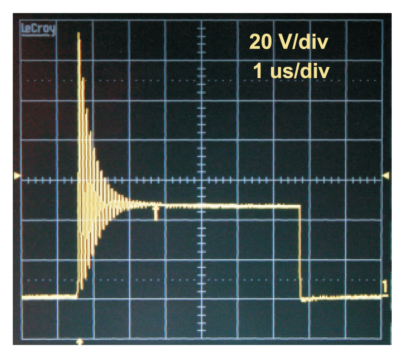
Figure 3: Flyback converter FET voltage waveform.
Figure 3 shows the FET voltage for a typical flyback converter. It is often a surprise to new designers to see how severe the converter ringing is, and how much extra stress is applied to the semiconductors relative to the ideal square-wave waveforms.
Almost all flyback converters apply a clamp circuit, or snubber circuit to the FET to prevent the ringing waveforms from destroying the device. Before this is done, however, it is a useful experiment to look at the ringing waveforms closely to learn more about them.
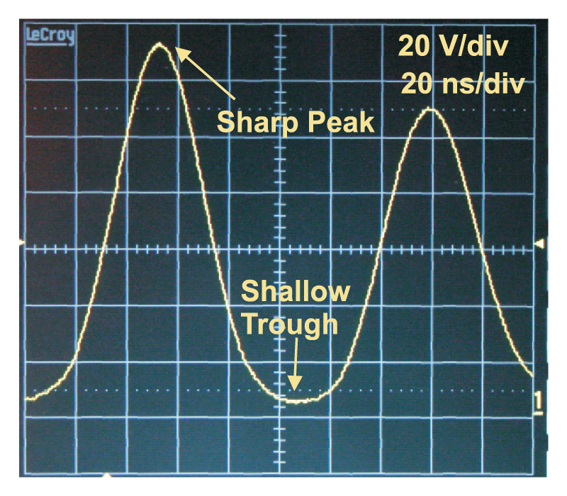
Figure 4: Flyback converter FET voltage waveform detail.
Figure 4 shows the same FET voltage waveform, zoomed in on the first two ringing cycles. The period of ringing is 110 ns, corresponding to 9 MHz. There is a general rule that this ringing frequency should be about two orders of magnitude (100 times) the switching frequency of the converter, or else the subsequent snubber dissipation of the ringing will be very lossy.
Notice that this waveform has an interesting characteristic distortion. At the top of the waveform, the peak is very sharp, corresponding to a high-frequency resonance. At the bottom of the waveform, the trough is very shallow, corresponding to a lower frequency resonance. The resonant frequency of the waveform is actually voltage dependent.
This particular waveform is a resonance between the leakage inductance of the transformer, board trace inductance, transformer capacitance, and the output capacitance of the FET. (Since the diode is on during this ringing, its capacitance is not involved in determining this waveform.) The voltage-dependent output capacitance of the FET is responsible for the distortion on the waveform.
If ever you see this kind of waveform in any of your power circuits, it means that the ringing is strongly dependent upon a semiconductor junction capacitance, rather than on a physical capacitive structure such as transformer windings or heatsink capacitance. This knowledge can help you troubleshoot your power supply, targeting the right component to reduce capacitance.
Measuring Waveforms without Touching the Circuit
The waveforms shown so far are produced by capacitances on the primary side of the converter, in the orders of tens of picofarads. As frequencies climb, and part sizes shrink, these capacitances can also reduce. We have to be very careful that any instrumentation connected to the converter does not materially affect the waveforms themselves. For many converter waveforms, attaching a scope probe affects the waveforms of the circuit, and in some cases, can cause converter failure. (It can also lead to the opposite effect – masking destructive waveforms that, without the instrumentation, would lead to failure.)
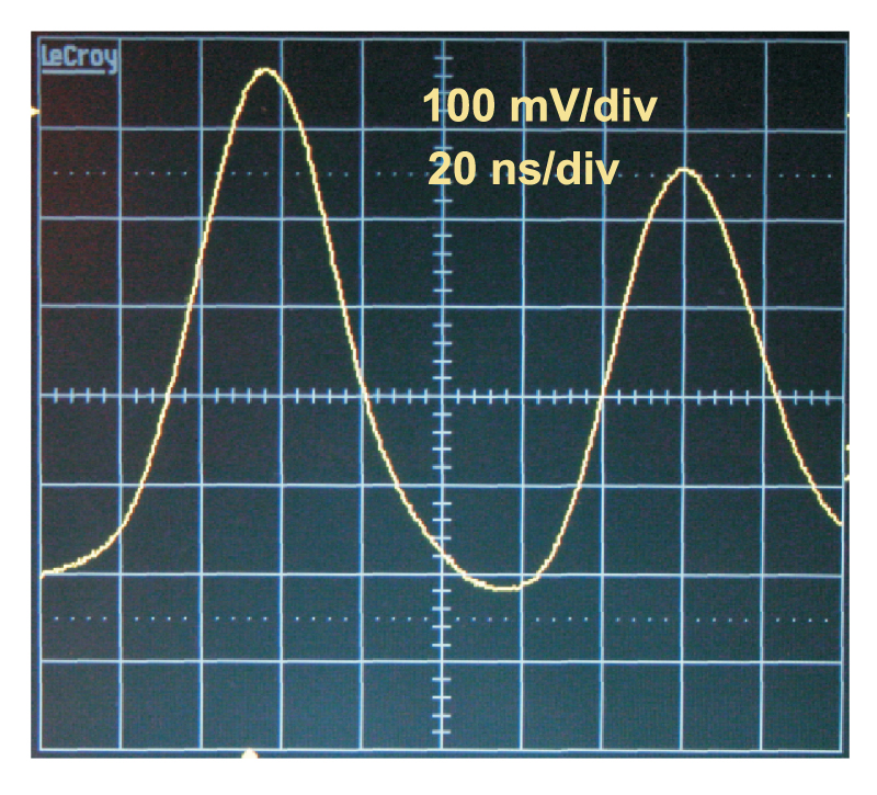
Figure 5: Expanded FET voltage measured without touching the circuit.
A technique to make sure we are not disturbing the circuit is to remove the probe tip and ground lead from the scope voltage probe, change the scale on the oscilloscope, and just hold the voltage probe near the component node we are trying to measure. For a FET drain voltage, the large area of the tab of power component will couple its signal to the scope probe very effectively. Figure 7 shows this test setup.
Figure 5 shows the FET drain waveform measured this way. Notice that voltage scale is now just 100 mV/division rather than the 20 V/division for Figure 4. You cannot use this technique to measure exact amplitudes, but you can see the waveshapes and frequencies involved.
In this case, the waveforms of Figures 4 and 5 are almost indistinguishable. There is just a slight shift in the ringing period to 105 ns due to the removal of the scope probe capacitance. After making this measurement, we can now rest assured that the instrumentation does not significantly affect our measurements in this case.
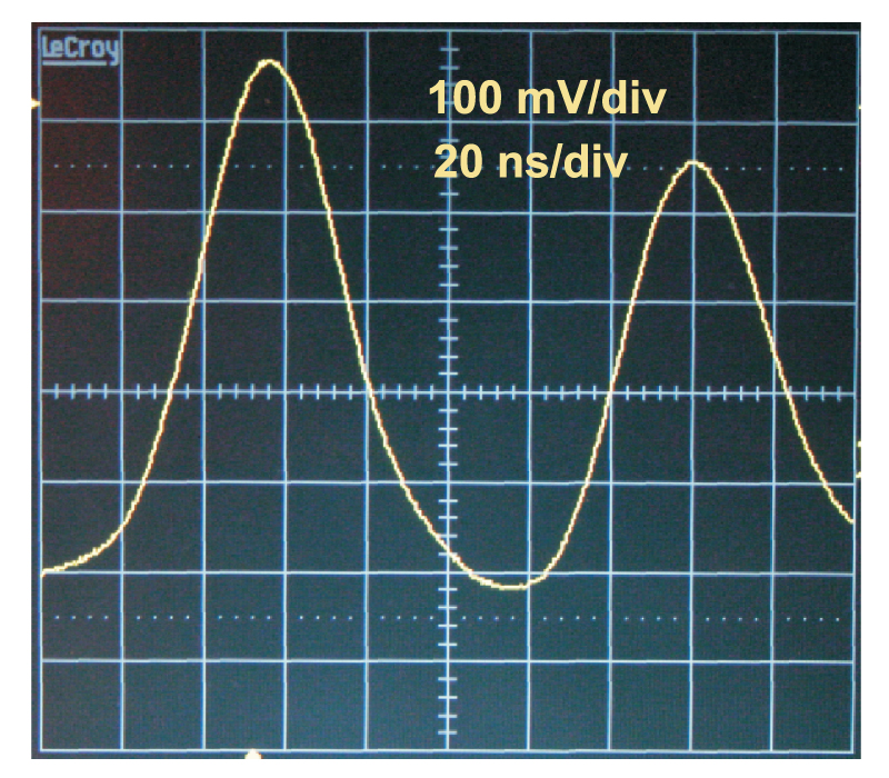
Figure 6: Flyback FET voltage in DCM, measured without touching the circuit.
Figure 6 shows the same circuit operating at lighter load. This waveform is again measured without touching the circuit with the instrumentation. There is an additional ringing period shown which corresponds to the converter entering discontinuous conduction mode (DCM). This is a much lower frequency, since it is caused by the magnetizing inductance of the transformer ringing with circuit capacitances.
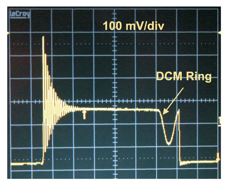
Figure 7: Measurement technique for voltage waveforms.
Figure 6 is a very characteristic signature of a DCM flyback. As you become more experienced in power supply design and their characteristic waveforms, the contactless measurement becomes a very powerful and rapid diagnosis tool. You can look at the waveforms of a hardware sample for which you may have no circuit diagrams, and quickly and safely be able to identify the type of converter involved, its mode of operation, and any potential problems in the waveforms.
Summary
Ringing waveforms contain much information about the design of a converter. Before you completely suppress them with snubbers and clamp circuits, they should be recorded and studied carefully. This will help you in the design of snubbers, in identifying dominant parasitic, and in protecting your circuit in all modes of operation.>
Transient events can give rise to additional circuit resonances, and you should always try to capture worst-case waveforms during test conditions other than steady state. Many circuit failure events occur during transients due to these additional stresses.
Always be careful when trying to measure very high frequency waveforms. The instrumentation itself can change the circuit. The contactless measurement technique described is a very useful diagnostic tool for switching power supplies, and you should practice this with your circuits.