


Introduction to the series on how to design a forward converter.
Introduction
This article begins a new series in which Dr. Ridley shows the multiple testing and revision steps needed to get a power supply from concept to a fully-working prototype.
Power Supply Development Time
Whenever I look at doing an off-line power supply development, I have a formula for calculating how long it will take. I lay out each step of the process, and estimate the maximum amount of time that each step might take. Then I double the result. After this, I am normally hard-pressed to finish on time.
Why does this happen? It’s because there are always unforeseen events that can drastically slow down the development process. After many years of working with switching power supplies, you learn that parts seldom behave exactly as you expect them to, and when designing for a rugged environment of line variations, surges, short-circuits, and temperature variations, you can never be sure how long things will take.
It is hard to explain to those new to power supply design exactly what can go wrong. It is also hard to explain to management why the project schedule estimate is so long, and why we might need three or more board turns to get such a “simple” circuit right. Part of the reason for this difficulty is that when solving the problems of a power supply, we are often in a hurry and rarely have time to fully document the steps involved in fixing problems. Later on, we forget exactly what happened to take so long.
I am guilty of following the same process. When working on a consulting design, or on a design for my own projects, the main objective is to be done as quickly as possible. Recently, however, I had a unique opportunity to take the time to fully document the process steps in going from a power supply that was already laid out and ready for testing, to getting the supply up to full power. In following this process, I encountered many events I had seen in the past, and never documented.
Power Supply Requirements
The specification for the power supply was as follows:
1. Output 1 – 35 VDC @ 10A isolated
2. Output 2 – 35 VDC @ 10 A isolated
3. Maximum power 350 W (only one output fully loaded at a time, application is for audio.)
4. Input – 180 – 265 AC
5. Power Topology: Two-switch forward
6. Controller: Digital controller from TI
The project was launched for several purposes. Firstly, I needed a bulk supply for an audio product which is currently running from a linear supply. Secondly, I had a digital designer who was eager to work for me for four months to try and learn some real-world power supply design. I have watched the promise of digital for over 20 years now, and felt is was finally time to see whether it could really work in a real-world product. And finally, I have always recognized the two-switch forward as the most rugged topology available, but never actually built one from scratch. It was time to learn the details of the topology first hand.
The optimistic goal of the project was to finish in plenty of time so that a second converter with the same specifications could be built to run from the one digital controller. I didn’t really expect this to happen in the given time frame, but it was kept as a goal. At the end of the project, I hoped to have a working prototype, learn a lot about digital controllers and their quirks, and to impart some knowledge on analog power design.
As is often the case in the power supply world, things didn’t quite work out as planned. At the end of the four months, I found that I still couldn’t program a digital controller (although I learned a lot), and a digital designer couldn’t possible learn enough about high-voltage analog design in such a short time. However, I learned a tremendous amount about our analog design process and why it remains a challenge after so many years. The digital designer returned to the world of low-power offline work, and he learned more about his digital algorithms but not, unfortunately, what makes the analog world go round.
Separation of Power and Control
The first major lesson when working with a digital controller is that the layout needs are totally different from the needs of the analog power stage. The digital part of the board requires fine-pitch traces, and at least a four-layer board. On the other hand, the power stage requires heavy copper for high-current traces, large trace separation for voltage breakdown requirements, and pleny of allowance for thermal management, and bulky magnetics. And, as we shall see later in this series, you must be able to rework the power board manually to arrive at a well-designed converter in the shortest amount of time.
I always work with just two layers for power supplie. I like to be able to see all of the traces on the top and bottom sides to ensure proper spacing for all components. I also like to have the ability to move a trace if necessary, and relocate critical components without having to layout a new circuit board.
In early development, the most practical thing to do is separate the controller and power stage into two boards with a connector between them. Digital control forces you to this approach. This is also an approach I have always taken for analog power development. A controller from one project is often very applicable for your next project, and can be taken as a partial pc board and interfaced with a new power stage. This can save a tremendous amount of time, and is easy to do if you have a clear delineation between power and control.
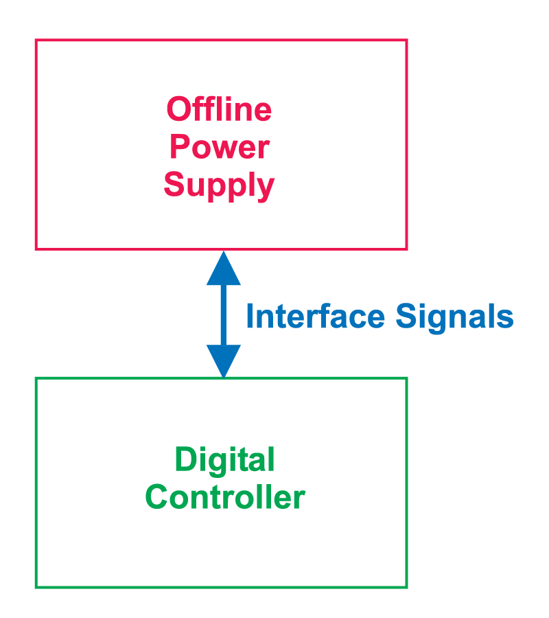
Figure 1: Separation of Power Circuit and Control Circuit with Interface Signals
During the development of most power converter, the control and power stage delineation becomes blurred with more and more communication from one to the other. The addition of ground planes confuses the line even more. This can lead to multiple problems with noise.
Ground and other PCB planes should be completely separate between the control board and power board. This is naturally achieved when the two boards are built separately, as is recommended for the early stages of digital control. This proper separation of the power and control boards will be discussed in more detail in the next article of this design series.
Full Schematic and Layout
The full schematic of the forward converter will be presented in the next article of this series. The power layout took about 1 month to complete, including the entry of all component footprints and placement of parts and traces. When working with existing parts databases, I usually expect this process to take me about two weeks. Less experienced designers can easily spend eight weeks on this process if starting from scratch.
The layout alone is a topic worthy of a complete series of articles. I won’t go over that in full detail in this series, and will concentrate instead on the issues involved in completing the design after the first layout was complete.
Debugging the Power Stage
The question that has troubled me the most about digital control has been the issue of debugging. After many years of solving power supply problems where you have to capture fleeting events, and track them down through power stage and controller waveforms, I have always wondered how on earth this can be done in conjunction with the development of software and digital controllers, which may also have bugs.
Finally, I think I have come to resolution of how this must be done. The answer is simple – the power stage must be fully debugged with an analog controller before the digital control is implemented! This is not a comfortable answer for the advocates of digital control. You must go through a complete analog design first, and then implement the digital and software aspects. It’s clear that the development time of this approach will be considerably longer than just analog control. So the digital control implementation must offer significant advantages to justify this extra time. For some systems it does, for some it doesn’t.
A big thing I learned about the difference of analog and digital designers is the way they think about their circuits and components, and there is a fundamental divide between the two. Digital controllers and microprocessors in general, have millions of transistors in their circuits. They are all expected to work within their specs, and work perfectly. When the software is complete, there should be no surprises. Designers do not expect the individual transistor circuits to misbehave.
In the analog power stage however, after many years experience, you learn to expect almost every aspect of the circuit to misbehave. Nothing is exactly the way it should be according to the textbooks or datasheets.
This will be clearly illustrated in the following parts of this series. A surprise to me in documenting the process was how many steps were involved – most of them involve events not to be found in any book or datasheet. There were several categories of problems that had to be resolved:
1. Failed components
2. Misconnected components
3. Component values
4. Unexpected operation in regions outside of the component specifications.
5. Layout
6. High-frequency parasitics and noise
7. Snubbers and clamp circuits
8. Mechanical
9. Magnetics
10. Control stability
In all, in moving the converter from the initial board layout to a full power prototype, there were a total of 85 process steps. That does not include full characterization of the power stage and control optimization. The work is ongoing, when I have time to get back to the bench. I would expect in excess of 200 steps by the time the converter is done and ready for production.
For me, with 30 years experience, these steps moved very rapidly since I had seen many of the phenomena before. It took a total of approximately two weeks to implement them all. For the inexperienced designer, many of these steps can take days or weeks to solve. Quite often, the project can never be completed since the solutions are hard to find without experience.
Summary
The key learnings of the first stage of the project:
1. There must be a clean separation of power stage and controller, whether using analog or digital control.
2. A digital designer cannot learn analog power stage design in four months
3. If you want your power supply to work with a digital controller, you must first debug it with an analog controller. You cannot take on both problems at once.
4. Resolving the power stage issues alone can be a very long process, and design experience is essential to expedite this.
In the next article of this series, I will begin describing the full schematic and the initial problems with getting the converter working
Further Reading
Power Supply Design Center Library