


Initial testing on a forward converter design.
Introduction
This article continues the series in which Dr. Ridley documents the processes involved in getting a power supply from the initial design to the full-power prototype. In part II, we focus on the interface between the power stage and controller, and getting the gate drive working properly.
Power Supply Development Testing
The results of initial testing are shown in this article for a two-switch forward converter. This was a project for which the initial prototype breadboard was complete, and it was time to apply control and power signals. As mentioned in the first article of this series, there were a total of 85 process steps involved in moving the power supply from the original non-working condition to a full power board. It would take too many articles to present every detail of each of these steps, so I will focus on the events which I have observed many times before in the industry.
Power Supply Requirements
The specification for the power supply was as follows:
Output 1 – 35 VDC @ 10A isolated
Output 2 – 35 VDC @ 10 A isolated
Maximum power 350 W (only one output fully loaded at a time, application is for audio.)
Input – 180 – 265 AC
Power Topology: Two-switch forward
Controller: Digital controller from TI
Power Stage and Control Interface Schematic
The full schematic of the power stage is shown in Figure 1, together with the signals for interfacing with the control circuit. The power stage was completely separated from the control so that each could be worked on individually, and layouts for each were independent. This is crucial for a digital power supply controller which needs fine-pitch layout versus the heavy copper suitable for the power stage.
It is quite common to find errors in either circuit that can require a new layout – keeping the power and control separate can greatly speed up the development process. For early testing, it is often a good idea to provide a connector between the two, with two separate boards.
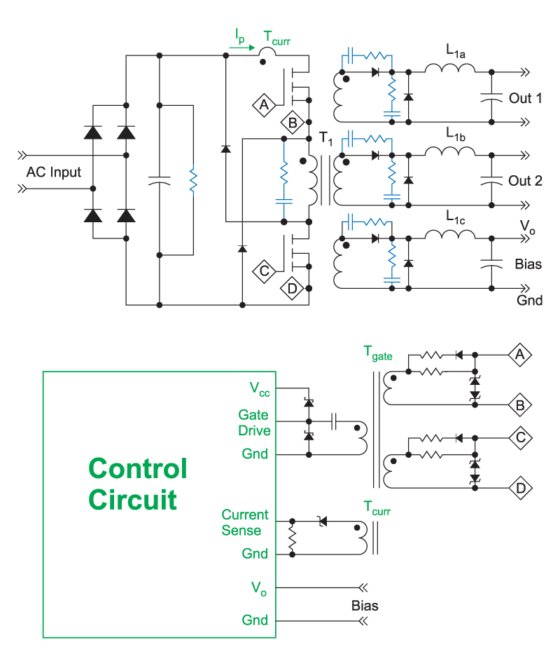
Figure 1: Power Stage and Control Interface Schematic
For high power work, using either digital or analog controllers, it is best to have only one ground connection between the control circuit and the power circuit. There should be no overlap of ground planes in order to prevent power currents from flowing near the control parts. A single point ground should be established between the two parts of the circuit.
The drive for the gate of an offline power supply should be galvanically isolated for both of the power FETs using a gate drive transformer as shown in Figure 1. This is much better than using an integrated high-side driver. A gate drive transformer has the advantage of providing negative gate voltage during the off-time which provides superior noise immunity from accidental turn on of the FET. A gate drive transformer is also much better during the development phase when power stage failures are likely to occur. If the high-voltage power FET is destroyed, the damage is usually limited to the secondary of the gate drive transformer, and the control circuit is left intact. This is crucial for finding the root cause of failures.
The current-sense network is also galvanically isolated. The current transformer network shown provides the cleanest signal for current sensing, and its wide bandwidth allows for protection of the power devices as we shall see later.
Event #1 Bypass Capacitors
The first problem encountered was that the digital controller simply did not work properly when hooked to the gate driver. The issue was tracked down to the lack of a bypass capacitor in the proper place for the gate-drive chip. The need for this was documented in the data sheet, but deeply buried in other information.
If you haven’t worked in power supply design before, adding bypass capacitors next to your integrated circuits is often just a formality. Quite often, they can be removed without any detrimental effect. However, they are crucial elements of power supply control circuits, especially when power FETs must be driven. Placement of all bypass capacitors for gate-drive outputs, clocks, references, and supply voltages must be very tight to the integrated circuits.
The lack of a gate-drive bypass capacitor also highlighted the difference in thinking of digital and analog engineers. The digital engineer’s immediate response to the oversight was to make another board before proceeding. The approach from most analog engineers would be to add a bypass capacitor next to the chip with two lengths of hookup wire and move on to the next test. Experienced power designers know there will be many such issues, and it is best to collect as many changes as possible and rework the PCB when the changes become unmanageable.
Event #2 Gate Drive Overheating
Once the bypass capacitors were properly placed, gate-drive waveforms at 200 kHz were obtained from the control chip. However, both the gate driver and the lower power FET overheated significantly, even with no power applied to the input of the power stage. The FETs were able to switch a resistive load, but something was not working properly.
led to another significant conclusion for me. An overheated and destroyed gate driver for a digital controller is a substantial repair problem. The high density drivers have pads on the bottom which, when surface mounted, remove the heat very effectively. However, this prevents you from mounting the driver in a socket. After many years experience in designing offline converters, you learn that failures of the control chip and the gate-drive chip are common events. When trying to track down failure mechanisms, it is not uncommon to burn through many chips in a day. If they have to be unsoldered, this can be a very tedious process, severely impacting development time.
At this point, the digital controller part of the project was put on hold. Clearly, it did not make sense to continue debugging the power stage at the same time as working with a digital controller. An analog control board from a previous project was substituted for the digital control to allow testing to continue. The clearly delineated separation of the control and power stage made this substation straightforward.
Only one of the FETs was hot with the gate drive applied. The waveforms on this FET are shown in Figure 2. There was a significant drop in the predicted voltage, but the waveform still looked reasonable if you are not familiar with normal FET operation.
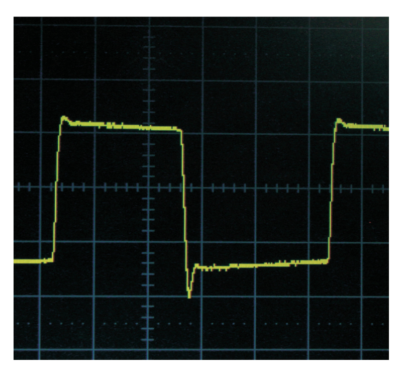
Figure 2: Gate Drive Waveforms with Damaged Gate
One indication that something is not right is that the waveform is very square. Upon being desoldered from the power board, the gate-to-source resistance was measured at 27 ohms when it should be an open circuit. The gate may have been damaged by static when handling or mounting to the board, or it may have been damaged upon arrival. It could also have happened when the power board and controller were connected together.
Notice the use of back-to-back zeners across the FETs. These were added after the failure was found, a normal precaution for offline converters. Figure 3 shows the proper gate waveforms after the FET was replaced. Notice the higher amplitude, and the curve of the top of the waveform. This is characteristic of the gate drive scheme chosen.
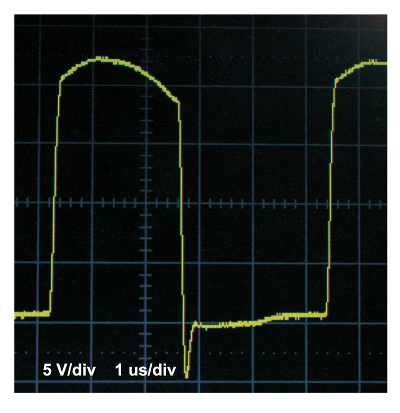
Figure 3: Normal Gate Drive Waveforms
Event #3 Driving Inductive Loads
The digital controller was replaced with a 3825 controller, one of the most rugged chips on the market. This is a good choice of controller to use to debug a power stage. In order to test the initial operation, the controller from another power supply design was used with wires jumping between the two boards. This allowed testing to rapidly continue without designing a special board.
The initial operation, however, was very unpredictable, with very narrow or missing gate pulses from the controller when connected to the transformer. This was due to a second common problem. Most bipolar technology control chips cannot provide the reactive current needed by a gate-drive transformer. The solution to the problem is shown in Figure 1 – schottky diodes must be added at the output of the gate signal to supply the reactive part of the current.
Other Early Mistakes
When hooking up the power stage with a substitute controller, several other mistakes were made.
#4.The supply voltage Vcc was mistakenly applied to the output of the controller. The 3825 had to be replaced.
#5.An auxiliary ramp summing circuit for current-mode control was applying a negative voltage to the current sense input. Nothing works according to the datasheet if you do this. This is a more common occurrence than you might think when hooking up low-voltage control circuits to high-voltage power stages.
The first of these mistakes was made after trying to achieve too much in one day. Working on power supplies requires a clear and fresh mind to avoid mistakes. In this case, it was easy to fix the controller since it was in a DIP socket. When power is being applied, though, working while tired can be dangerous, destructive, and often very time-consuming.
Summary
The first phase of this project showed up numerous errors and failures that are difficult to predict and anticipate. This is normal in power supply development, and such events must be budgeted in the schedule. If you are a manager, pushing your engineers to work harder and longer hours is not the path to better results. The development and testing of a power supply must be a deliberate and methodical process with sufficient time allocated to work efficiently with a clear head.
Switching to an analog controller during the debugging process was clearly a necessary step to get the power stage operating properly. This eliminated unknowns of a very complicated component, and made replacement after failures fast and straightforward.
In the next phase of this article, power is applied and the process of debugging continues.