


Further testing on the forward converter.
Introduction
This article continues the series in which Dr. Ridley documents the processes involved in getting a power supply from the initial design to the full-power prototype. In part III, initial power is applied to the circuit with a resistive load to verify proper operation of the primary circuitry.
Power Supply Testing with Analog Controller
In the previous article of this series, several problems were found on the control board prior to applying power to the input. The first important lesson was that trying to debug a digital controller at the same time as trying to debug a power stage was not a reasonable approach. The digital controller was replaced with a standard analog controller in order to debug the power stage while minimizing the number of variables.
After several years of power supply design, you become quickly aware that you cannot “breadboard” designs with proto-boards and long wires. Critical noise-sensitive areas MUST be laid out on a PCB to provide minimal path lengths for high frequency connections, and ground planes for shielding. In all projects, you want to minimize the development times. Decisions must be made about whether to stop testing and return to board layout, or provide compromise interim solutions in order to collect data as quickly as possible. One trick I have used frequently is to build power supply test circuits from a collection of previously-designed printed-circuit boards. For this project, a control circuit containing a 3825 controller was cut out of a large PC board, and connected to the power circuit after removing the digital controller parts. This allowed testing to continue after just a few hours work.
Applying Bulk Power to the Circuit
The schematic of the power stage is shown in Figure 1, together with the signals for interfacing with the control circuit. Snubbers are omitted from Figure 1 for clarity. (This circuit was shown in full in the previous article in this magazine [1].)
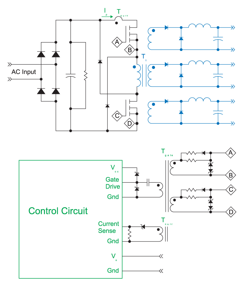
Figure 1: Power stage and control interface schematic. Snubbers are omitted for clarity. The power transformer and secondary circuits are highlighted in blue – these will be removed for initial power stage testing.
After testing the gate drive waveforms, and correcting circuit problems in part II of this article, power was applied to the circuit. There are a couple of choices for doing this, one of which is to use a DC bench power supply to apply a fixed voltage. Such a supply must be capable of providing high voltages, up to 400 VDC, and high currents in order to operate at low line and full load. For a 350 W design, a 1 kW bench supply is typically needed, which is expensive, bulky, and potentially hazardous.
I always prefer working directly from an AC source at the very beginning of a project. This will often bring out problems with the AC connections that you do not want to delay finding until later in the project. An isolated AC source provides a good compromise of safety and instrumentation options, as discussed in [2].
Figure 2 shows the circuit for the initial power testing. The transformer of the power supply was removed, and replaced with a power resistor. This allows us to test the following elements of the power supply:
Instrumentation connections and grounding
Gate drive waveforms with voltage applied to FET
Turn-on thresholds and gate drive levels
Current sensing circuits
FET operation with voltage applied
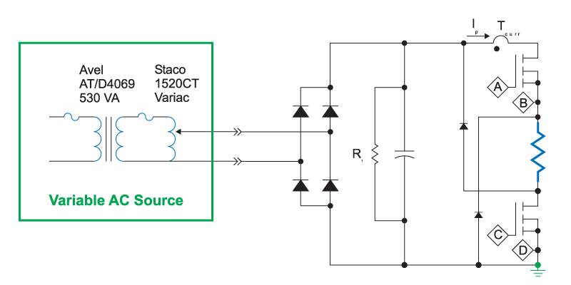
Figure 2: Power stage schematic with transformer and secondaries replaced with a test resistor.
The resistive testing of Figure 2 is something that I always do during the initial test phase of a power supply, regardless of the topology. There are simply too many variables involved when adding all of the magnetics and secondary elements to be able to initially verify that primary switching is operating properly.
Removable Magnetics
I have learned over the years that simple removal and replacement of magnetics is essential for rapid development. Regardless of the power level and topology used, it is highly likely that you will try multiple different versions of magnetics during the development process in order to optimize the design. If the parts can be quickly changed, this saves a lot of time and wear-and-tear on the PCB.
Figure 3 shows sockets inserted into a circuit board, ready for a transformer to be plugged in. Rugged sockets are available that provide solid connections with high current-carrying capability. The Mil-max sockets shown can be used for up to 10A for testing. (Once the magnetics design is finalized, you can always add solder to the sockets to improve measured efficiency.) These particular sockets can also be used for plugging in test resistors.
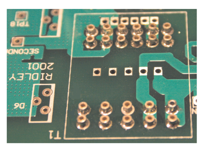
Figure 3: Socketed magnetics speed up the development process and allow fast iterations in the design.
For higher current applications, you can use PCB inserts that allow you to bolt foil and bus-bar terminations to the board with very low connection resistance on the secondary, and still use sockets on the primary where currents are lower.
Initial Resistive Power Testing Waveforms
Figure 4 shows the gate drive waveform with voltage applied to the power stage. The waveform is almost the same as that without voltage applied, with the exception of the small region of switching due to the Miller threshold event. Once the FET begins switching, the drain voltage must fall, and the gate drive must provide current to charge the gate-to-drain capacitance.
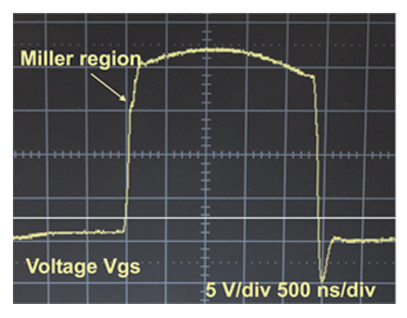
Figure 4: Gate drive waveform with resistive load of 160 Ohms. Note the Miller threshold region showing the switching level.
The Miller threshold region of the waveform is very useful for identifying at which voltage the FET is actually switching. There should be plenty of drive available to provide several volts in excess of this threshold to ensure that the FET is turned fully on. For a transformer-coupled gate drive, the minimum voltage is applied at maximum duty cycle, which is shown in Figure 4.
Figure 5 shows the voltage and current waveforms of the FET. With a resistive load, both waveforms are close to square waves. It is always good to check the current sense network output under these conditions to make sure the protection is going to be available when the magnetics and secondaries are connected.
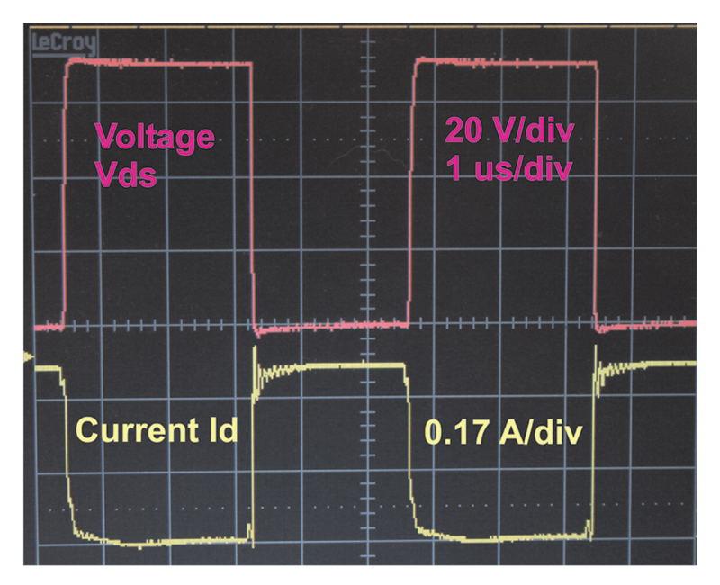
Figure 5: FET voltage and current waveforms. The current waveform is observed using the current transformer circuit.
Using a resistive load of 160 ohms, the power supply was tested at up to 100 V dc input. This voltage was increased to 160 V with a 27 k resistor. Further testing could also be done at full input line voltages, taking care not to exceed the power dissipation capacity of the loading resistor. It is worthwhile doing this high-voltage testing with a resistor since it will show any voltage breakdown problems that may occur.
Failures and Build Errors Found
Event #6 Shorted Control Board Connection
After connecting the analog control board to the main power stage, control chip overheating was discovered, and several chips had to be replaced. The root cause was traced back to a washer shorting a PCB pad to ground. Mechanical shorts are common events in power supply construction. It is only when you assemble all the three dimensional parts that some mechanical clearance problems become apparent in a circuit. I have seen this kind of problem numerous times over the years at all different stages of production.
Event #7 Current Transformer Wired Backwards
When power was applied to the circuit, the initial current waveform was missing from the current transformer network. The root cause of this was traced to a wrong-polarity connection of the primary of the transformer. This may seem like a rudimentary error, but it is very common during the prototype and pre-production phase of design to have a polarity error in the custom magnetics designs.
Event #8 Input Capacitor Bleed Resistor Omitted
Very few papers talking about topologies discuss the need for the resistor R1 in Figure 1. This resistor is intended to discharge the input capacitor once the power supply is turned off. It is often tempting to omit the resistor since it increases dissipation and lowers the efficiency of the power stage. However, once you start testing, and you encounter failures, the value of the resistor soon becomes apparent. Holding a soldering iron in your hand, and confronting a capacitor charged to several hundred volts is not a desirable situation.
Make sure you put this resistor on your circuit for the development stage, even if you intend to remove it later on if you have a control chip that claims to provide the discharge path. If the control chip fails, you want to be sure that the input capacitor is fully discharged before working on the circuit.
Summary
Initial power should be applied to your power circuit with the transformer and secondaries disconnected, and replaced with a power resistor. This allows you to ensure that your ac source and instrumentation are properly connected, and that gate drives, current sensing, and other primary circuits are working properly before starting to deal with the complexities of magnetic design.
Magnetics should always be easy to remove from the circuit in order to try different designs later in your development process. In this article, socketed magnetics allowed the easy substitution of a resistor for initial testing.
In the next article of this series, the magnetics will be placed into the circuit.
References
- Join our LinkedIn group titled “Power Supply Design Center”. Noncommercial site with over 7000 helpful members with lots of theoretical and practical experience.
- For power supply hands-on training, please sign up for our workshops.
- “Power Supply Development Diary Part II”, Ray Ridley, Power Systems Design Magazine, April 2010.
- “Testing Offline Power Supplies”, Ray Ridley, Power Systems Design Magazine, January/February 2010.
- Design articles at the design center library at www.ridleyengineering.com