


Snubber and clamp design for a forward converter.
Introduction
This article continues the series in which Dr. Ridley documents the processes involved in taking a power supply from the initial design to the full-power prototype. In part V, attention is turned to the secondary side of the converter, where snubbers and clamps are added to protect the output rectifiers.
Secondary Catch Diode Ringing Voltage
In Part IV of this series of articles [1], the primary voltage spikes on the switching FETs were properly controlled with improved layout and high-frequency bypass capacitors. This greatly improved the ruggedness of the converter.
Voltage spikes and ringing can also be seen on the secondary of the converter. Figure 1 shows the ringing across the catch diode with 100 VAC applied to the primary of the converter (maximum voltage rating is 280 VAC). This ringing must be suppressed before higher voltages can be applied to the converter. A peak voltage of 175 V is seen at the leading edge of the waveform, more than three times higher than the anticipated square wave voltage of 50 V. If this is not controlled, the secondary rectifiers will fail when full voltage is applied.
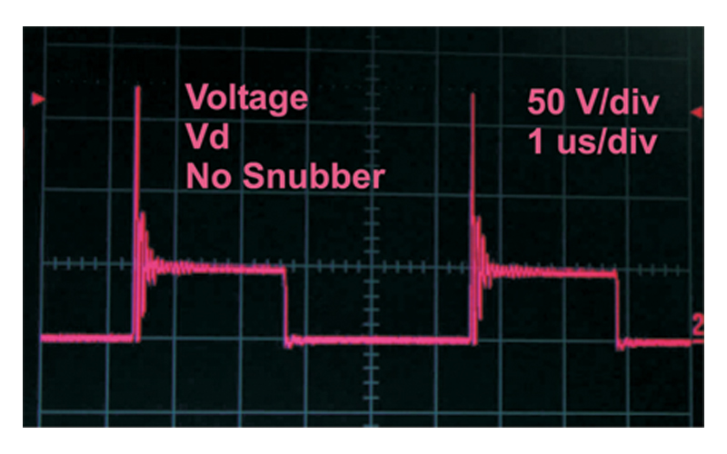
Figure 1: Secondary catch diode voltage waveform, VD, with 100 VAC applied and no snubber
Secondary Catch Diode RCD Clamp Network
A simple RC snubber applied across the catch diode of the converter is not able to sufficiently control the peak of the ringing waveform. Instead, an RCD clamp is used, as shown in the schematic of Figure 2.
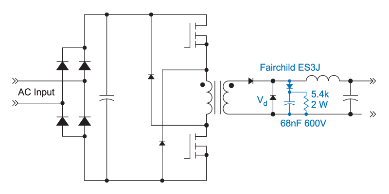
Figure 2: Schematic showing location of Secondary RCD clamp. Only one of the three outputs is shown for clarity.
RCD clamps are most often applied on the primary of an offline converter where the peak voltage must be tightly regulated to avoid failures. However, they can also be used on converter secondaries, especially when the output voltages. The clamp diode and capacitor must be placed very close to the terminals of the catch diode for maximum effectiveness.
Figure 3 shows the effectiveness of a well-designed RCD clamp. The peak voltage is reduced to 90 V from 175 V.
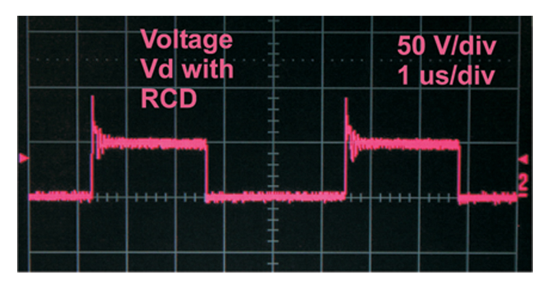
Figure 3: Secondary catch diode voltage waveform with 100 VAC applied and with RCD clamp
Design of the components is quite straightforward. The capacitor is chosen so that it retains a relatively constant voltage over each switching cycle. A 600 V multilayer ceramic capacitor was used with a value of 68nF.
The diode of the clamp needs to be either a schottky, or a fast recovery type. In this converter, a Fairchild 3A ultrafast diode with a rating of 600 V was used (ES3J).
The value of the RCD resistor can be selected according to the process in [2], or can be chosen experimentally. The smaller the value of the resistor, the harder the voltage across the diode is clamped, at the expense of higher dissipation. Full analysis of the RCD snubber can be found in [2]. Although this article is specifically for the flyback converter, the procedure is the same.
The power dissipation in the RCD clamp can be reduced by connecting the resistor to the output voltage, instead of ground, as shown in Figure 4. Depending on the topology used, this can result in significant power savings. For the two-switch forward, approximately 40% of the energy is recovered at low line with this alternate connection. With this approach, the RCD clamp dissipates just above 1 W when the power supply operates at an output of around 400 W.
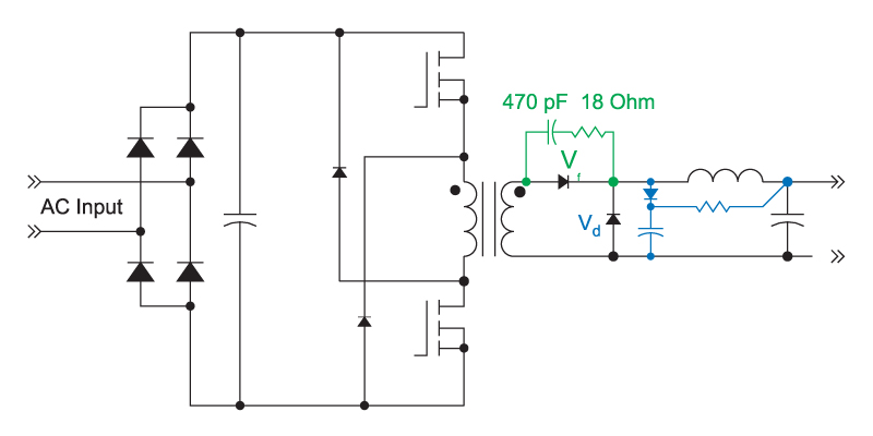
Figure 4: Schematic Showing Improved RCD clamp with lower dissipation, and RC Snubber added to protect the forward diode.
For very high power converters, you may also consider using a switching converter to discharge the clamp voltage. Active clamp networks can also be used but these add complexity and are beyond the scope of this article.
Secondary Forward Diode Waveform
The RCD clamp only protects the catch diode of the forward converter. It is also necessary to add a snubber across the forward diode on each of the converter outputs. Figure 5 shows the waveform across the forward diode before a snubber is added. The peak voltage spike seen is approximately twice the square wave value. A simple RC snubber is sufficient to reduce this spike to safe levels, as shown in Figure 6. The RC network is placed directly across the forward diode, as shown in Figure 4. The design process for these components is given in [2].
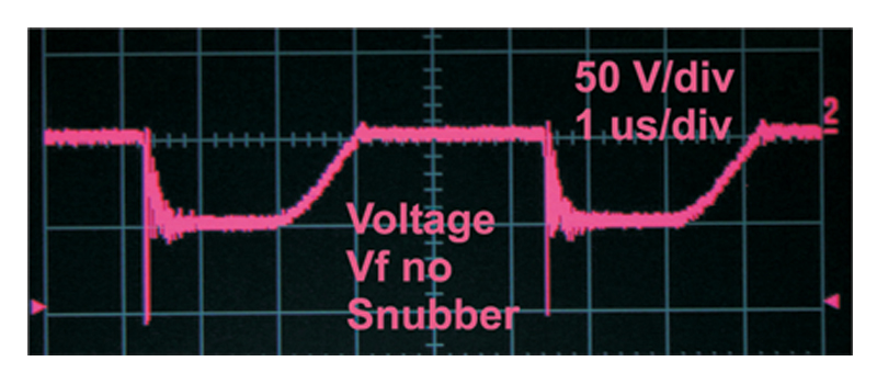
Figure 5: Secondary forward diode voltage waveform with 100 VAC applied and no snubber Figure 6: Secondary forward diode voltage waveform with 100 VAC applied and RC snubber.
The design of the RCD clamp and the RC snubber must be replicated on the second main output of the power supply. The lower power outputs can usually be designed with RC snubbers only. However, it is important that even the lowest output power diodes be checked for ringing and properly protected if you want to maximize the reliability of your converter.
Summary
The diodes on the output of the forward converter are protected with a combination of RCD clamps, and RC snubbers. It is important that every power diode be protected with a snubber or clamp, and tested under all conditions to ensure that the peak voltage ratings of all devices are never exceeded.
So far, the power stage testing has followed this order:
1. Check gate drive circuit waveforms.
2. Test primary circuit with resistive load.
3. Insert magnetics into circuit and verify low-voltage waveforms.
4. Design proper voltage clamps on primary switches.
5. Design proper voltage clamps and snubbers for secondary diodes.
All testing has been carried out at a relatively low input voltage – just 40% of the rated input. Before higher voltage testing is done, the overcurrent protection of the power supply must be thoroughly tested. This will be the topic of the next article in this series.
References
- Join our LinkedIn group titled “Power Supply Design Center”. Noncommercial site with over 7000 helpful members with lots of theoretical and practical experience.
- For power supply hands-on training, please sign up for our workshops.