


Initial full-power testing of the forward converter.
Introduction
This article continues the series in which Dr. Ridley documents the processes involved in taking a power supply from the initial design to the full-power prototype. In Part VII, the converter will operate at full power, and cross-regulation of the outputs will be tested.
Full Power Testing
As a reminder from Part I of this series of articles, the power supply specifications are as follows:
1. Output 1 – 35 VDC @ 10A isolated
2. Output 2 – 35 VDC @ 10 A isolated
3. Output 3 – Bias Supply, 12 W fixed load, ground referenced.
4. Maximum power 350 W (only one output fully loaded at a time, application is for audio.)
5. Input – 180 – 265 AC
Regulation on the outputs is not tightly specified. This design was for an audio application to replace an unregulated power supply with a 50/60 Hz transformer. As you can see in Figure 1, the three outputs of the converter are all on one common inductor core. This coupled-inductor approach provides the best regulation of the outputs, and is a very useful technique. With both outputs isolated, the intent was to regulate the converter from the grounded bias output.
Notice that the turns ratios on the inductor must be exactly equal to the secondary turns ratios on the transformer in order for this scheme to work properly.
Prediction of cross-regulation cannot be done theoretically, and the first major task after getting all of the semiconductors protected and prototype flaws fixed is to test the output regulation under all conditions.
Unprotected Diode Failure
The last three parts of this series [1] described how the semiconductors were protected with clamps, snubbers, and proper current limiting to make the converter rugged. This was implemented with low voltage applied to the converter. After this protection was properly designed, the converter was ready for full power testing.
Unfortunately, when the input voltage was raised to 200 VAC with 300 W load applied to the output , there was a failure. The primary switch current climbed rapidly each time the switch was turned on, there were indications of magnetics saturation (limited by the current-limit circuit), and the output diode on the bias winding became extremely hot.
There are a total of six output diodes in this converter, two for each output. On the main outputs, an RCD clamp protected the catch diode, and an RC snubber sufficed to protect the forward diode, as shown in Figure 1.
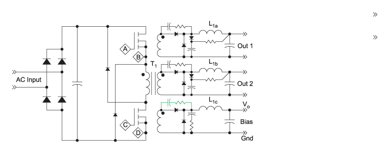
Figure 1: Three-output forward converter with secondary snubbers and clamps.
The catch diode on the bias output (15 V and 12 W only) had an RC snubber, but the snubber across the forward diode, shown in green in Figure 1, was omitted. It was realized that the RC snubber had not been placed on the board. The low power of the output led to a common trap—not fully testing that particular diode, and assuming that the overrating of the diode was sufficient to protect it.
Figure 2 shows the ringing across the forward diode on the bias winding output with approximately 100 VAC applied to the primary of the converter (maximum voltage rating is 280 VAC). A peak voltage of 160 V is seen on the waveform, more than five times higher than the anticipated square wave voltage of 35 V.
This is a common mistake made in many production designs. The bias windings are often very low power, and high voltage diodes are commonly used, without any snubbers. However, the peak ringing voltages can be extremely high (as seen here), and must be properly suppressed.
Figure 3 shows the diode voltage after an RC snubber was added. Dissipation in the snubber was very low, less than ¼ W, but the snubber was very effective at suppressing the ringing. Once this diode was protected properly, there were no more failures during this phase of testing.
It is interesting to note that the schottky diode fails in short-circuit mode. The current limiting in the primary prevents enough power being delivered to fuse the component. You should always remember that schottkys are not at all tolerant of overvoltage, and there should always be a good margin for a rugged design. Just to reiterate – make sure you test every semiconductor for peak voltage and current stress, regardless of how far within the ratings they may seem to be.
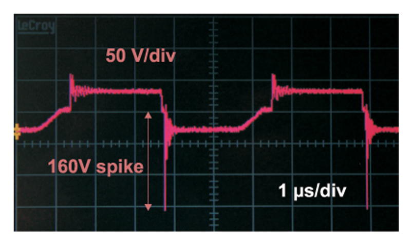
Figure 2: Secondary forward diode voltage waveform, VD, with 100 VAC applied and no snubber
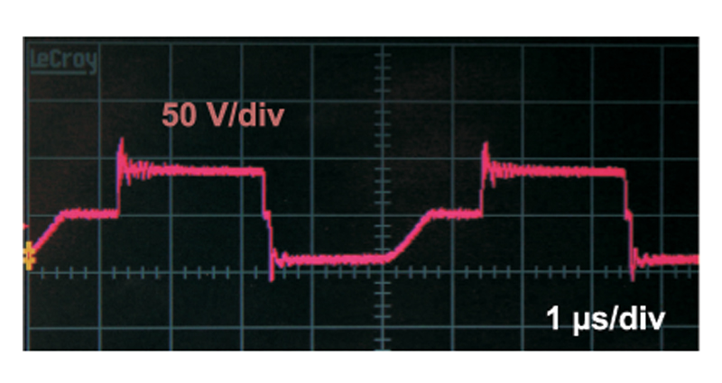
Figure 3: Secondary forward diode voltage waveform, VD, with 100 VAC applied, RC snubber
Power Supply Cross-Regulation Testing
The power supply was run with a fixed 12 W load on the bias winding. One of the main outputs was kept constant at about 25 W, and the load on the other output was varied from 1 W to 300 W. The converter was regulated from the bias winding, which was kept constant at 16.1 V. This process was then repeated with the other output loaded.
Figure 4 shows the cross-regulation curve for the two main outputs. The data is good – from 26W output to 300 W output, the variation in the output voltage is kept below 3%. For this particular application, this is more than sufficient, and certainly better than the previous unregulated power supply. Getting good cross-regulation is crucial to designing an effective switching power supply. This allows you to have multiple isolated output voltages without the complication and expense of isolated feedback networks, and post-regulators.
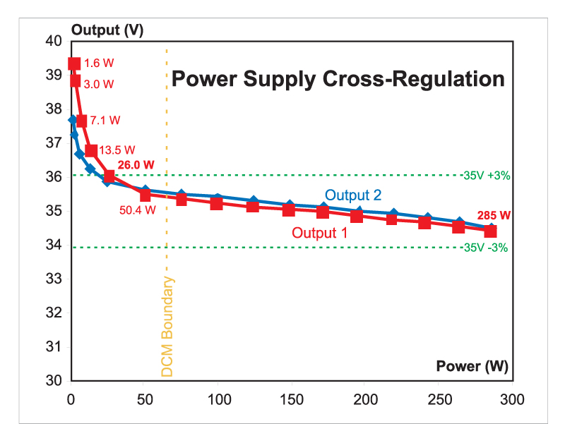
Figure 4: Power supply cross-regulation data. Bias output = 12W, main output = 1-300 W, second output = 26W.
The regulation curves of Figure 4 are typical for coupled-inductor designs, either flyback or forward derived. With well-designed magnetics, the output regulation will be very good from about 10% load to full load. At much lighter load, you can see that the curves turn upwards, and light-load regulation is not as good.
Notice, however, that good regulation is achieved even across the boundary of DCM operation, shown by the gold line in Figure 4. If you do not implement coupled inductors on the outputs, the cross-regulation if one of the outputs enters DCM is very poor.
Magnetics Winding Arrangement
For this converter, good cross-regulation was achieved due to the choice of winding arrangements in the magnetics elements. Figure 5 shows how the windings were arranged in the transformer. The main power outputs were either side of the primary, and the bias output was placed on the outside of the windings. The same arrangement was used in the inductor, with the omission of the primary winding.
The two high-power secondaries are not symmetric with each other in this arrangement, and the effect of this can be seen in the cross-regulation data. The red curve of Figure 4 loses regulation at a heavier load than the blue curve. The explanation for this is not well understood. In fact, it is hard to find many papers on coupled-inductor output regulation for the simple reason that you cannot write equations for how the outputs behave at light loads. There are so many parasitic elements involved in the switching process, and so many nonlinearities that come into play at light load, that proper analysis is impossible.
The only way to know how your converter will perform is to make extensive measurements on multiple prototypes under a wide array of different loads, input line, and temperature, to get statistical data on the regulation performance. Sometimes it is necessary to add a small fixed load to keep the outputs regulated at lighter loads. We will encounter analytical difficulties in predicting performance again later when looking at the small-signal characteristics of the coupled-inductor power supply.
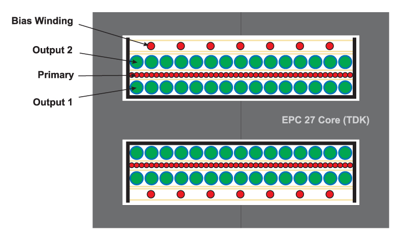
Figure 5: Transformer winding layout for good cross-regulation on EPC 27 core. The coupled-inductor winding has the same layout without the primary winding.
Summary
When testing the circuit at full power, there was a diode failure. This occurred on the low-power output schottky diode, which appeared to have plenty of derating for a 16 V output (diode rating was 200 V, 20 A). You should remember that every single output rectifier must be tested for peak stress, and then protected accordingly. These steps are often overlooked.
With proper protection in place on the final diode, the converter was run at full power. The power outputs were regulated +/-3% from full load down to about 8% load. This enables the topology to be used without any isolated feedback networks from the main power output, and without any post-regulator circuits. This is the strength of the coupled-inductor topology with good magnetics design.
References
- Join our LinkedIn group titled “Power Supply Design Center”. Noncommercial site with over 7000 helpful members with lots of theoretical and practical experience.
- For power supply hands-on training, please sign up for our workshops.