Testing and development schedule for the forward converter.
Introduction
This article continues the series in which Dr. Ridley documents the processes involved in taking a power supply from the initial design to the full-power prototype. In Part VIII, the prototype power supply is connected to a real system load and several issues are encountered.
Power Supply Design Schedule
So far, this series of articles has taken 7 months to present [1]. The actual uninterrupted time spent on the power supply testing and redesign was approximately 160 hours, following the initial completion of the PC board. Many issues have been resolved. Three iterations of the output inductor and four iterations of the power transformer have been built.
There are still issues remaining to be tested, including thermal performance, EMI, and proper control loop design. An estimated 100 hours of testing and data collection will be needed for this phase.
The hours that you will need for your project will vary significantly from this, depending on many factors:
1. How much power is being processed.
2. Input voltage range.
3. Design experience level.
4. Prior experience with the specific technology and topology chosen.
I have observed in the past that a good power supply designer will be able to get to production with perhaps three iterations of the printed circuit board. The first iteration should catch the critical issues that compromise the ruggedness of the power supply. As much data as possible should be collected from each board.
The second iteration of the board should be near production-level, depending on the extent of changes needed. The second board will typically be used for thorough thermal testing, EMI testing, and system testing.
The final board will fix any issues encountered to produce a manufactured product. Only minor changes should be needed on the final iteration.
PC board design time can be very variable. For the best designs, the power supply design engineer is intimately involved in the layout process, physically placing all of the critical components manually, and specifying the critical layout paths, power planes, and spacing.
System Testing
At this stage of the design, the power supply has been tested at full load, and across the full range of input line. Many changes have been made to the board to address the kind of issues that arise with virtually all switching power supplies running off-line. Most of the issues have been related to the first 200 ns of turn-on of the switch. Controlling overcurrent and overvoltage are paramount to making the power supply rugged. This applies to just about every power supply that is developed.
This is a reasonable point in the project to stop and implement a new PC board design. However, I have always found it very valuable to do preliminary testing with the real system as early as possible. There are always unpredictable issues that can be encountered.
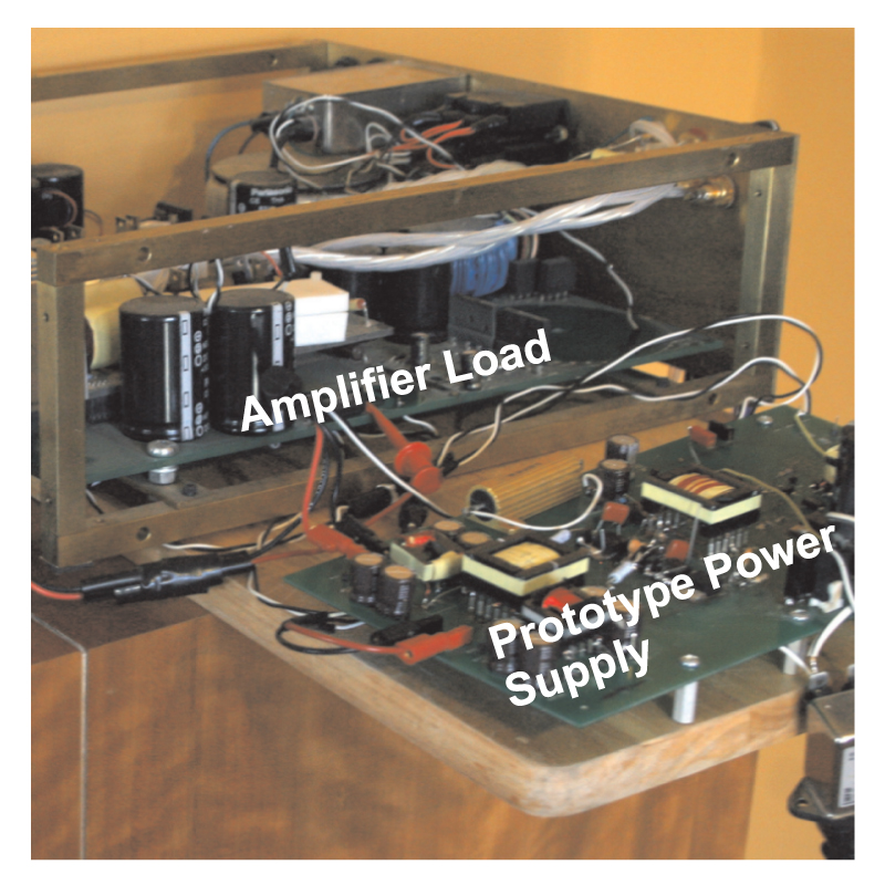
Figure 1 shows the prototype power supply connected to a power amplifier, the intended load. Remember this is a Revision 1 board, designed for stand-alone testing, so there are lots of wires to connect power supply and load. It is not uncommon for the early prototype to look distinctly low-tech, which sometimes alarms engineering managers who lack experience in power. While the setup is not particularly attractive, there is great value in performing this kind of testing early on in the power supply development.
Several issues were encountered in this project:
1. Power supply would not start when connected with low-impedance source and real load.
2. RCD clamp needed redesign.
3. Common-mode EMI interfered with amplifier circuitry, resulting in audible noise.
4. Actual load requirements were significantly lower than original specification.
Figure 1: First-pass PC Board Connected to System Load
Power Supply Would Not Start RCD Clamp Redesign
When the prototype power supply was first connected to its load, an immediate problem was encountered – the power supply would not start. There are two factors leading to this. Firstly, the power supply was being plugged into a very stiff input source, without a variac and power transformer presenting impedance at the input. Secondly, the load has significant internal capacitance, and this looks like a short circuit to the power supply when it first starts.
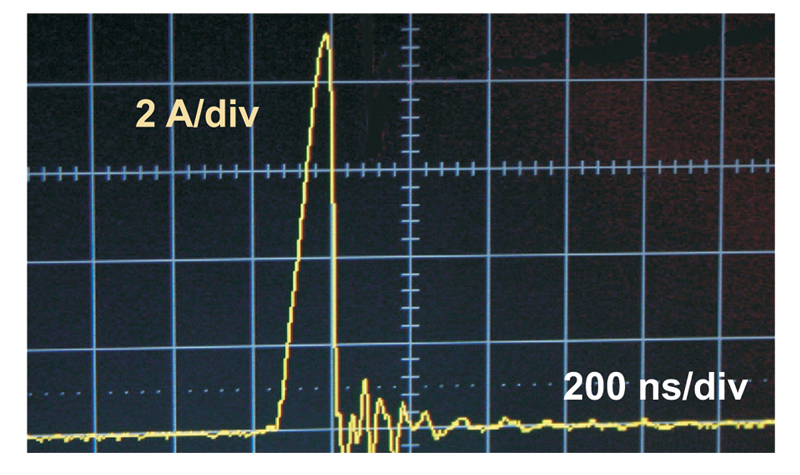
The main problem was the rapid application of input power. The observed primary current on the first cycle of operation was observed to be very high, as shown in Figure 2. This current looks very similar to the short-circuit current observed earlier in testing, and it was initially suspected that there was a short-circuit in the power supply. However, none were found, but the initial pulse of current continued to trip the second level of current limiting in the UC3825 control chip, initiating a soft-start delay.
After a day of testing, the problem was finally found to be an issue with the RCD snubber on the secondary of the converter. At turn-on, the two secondary RCD clamp capacitors (68 nF each) are completely uncharged. They must be charged up to the reflected input voltage on the secondary, and this results in the high current path shown in red in Figure 3. It only takes a couple of cycles to fully charge this capacitor, but if soft-start is initiated, the capacitor may have discharged again and the converter stays in a hiccup mode of operation with just a single pulse provided on an occasional basis. This is a drawback of the RCD snubber on the secondary side; it must be charged before it can begin to operate properly. Once charged, it has the advantage that there is no turn-on current spike due to this clamp, and it works very effectively.
In this case, the solution was to reduce the value of the RCD capacitor down to 4700 pF, a reduction of more than ten times.
Notice, however, that this will not fix the problem for every power supply. It depends on the input voltage, leakage inductance of the transformer (lower leakage results in a higher spike), and the rate of application of input voltage. This is yet another problem encountered during the first 200 ns of switch turn-on. It did not show up in earlier testing since the rise time of the input voltage was limited by the series impedance of an isolation transformer and a variac. [3]
Figure 2: Initial Primary Current with Discharged RCD Clamp Capacitor. Figure 3: Main Output RCD Clamps.
EMI Components
The next issue encountered is with EMI. The output noise on the power supply interacted with the load system and its grounding, resulting in audible noise from the output of the system. I have been on many consulting jobs where this was a major issue, and it can often be expected with switching power supplies.
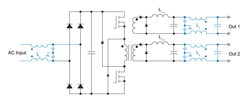
Space had been designed on the power supply board to accommodate a second stage filter [2], but I often like to design both a common-mode, and differential-mode filter in the same element for the outputs of a power supply. Figure 4 shows the common-mode filters which were added to the power supply on both the main outputs, and the input line. Once these were added, the measured output ripple was substantially attenuated by the differential- mode action of the filter. The common-mode action of the filter eliminated the noise from the amplifier.
Only when the chassis ground was connected to all the filters was the noise eliminated. This does not, however, always fix system noise. Sometimes the chassis ground itself can be corrupted with noise, so it is very valuable to conduct this level of system testing before the next iteration of the PC board. It gives a much higher level of confidence for final system integration.
Figure 4: Common-mode Filtering Added to Input Line and Outputs
Specification Revisited
The final issue encountered in the system was something that happens time and again in our industry. The power supply load was not the same as the original specification. In this case, the actual load was considerably less than the original 350 W anticipated. Electronics systems designers are notorious for overestimating the load current actually required. (Although, of course, it is sometimes underestimated, and that can present much more of a problem to the power supply designer.)
This is another great advantage of doing the real load test early in the design. The system designers may not be ready for your power supply, and they may balk at giving you a system to test, but you finally get to measure the real current requirements for yourself, and confirm that your design is adequate.
In this case, the system testing presents an opportunity for a major redesign which will save parts and money. Four outputs are needed for the amplifier, the original intent being to do this with two separate supplies. However, given the quality of the cross-regulation, and the lowered output requirements of the real system, there is the possibility of designing a four-output power supply using the coupled inductor.
This is a major change to the design, and one which presents a significant layout challenge. Total layout time for the new board was 55 hours.
Changes like this are very common in the power supply industry. You have to remain flexible, and have technology and circuits available to rapidly respond to changing user needs. The specification for a power supply is a living document, and something that is never really complete until the power supply is in production.
Summary
When developing a switching power supply, it is important to test the supply with the real load. If possible, you should do this before the second iteration of a PCB since several changes can be anticipated as a result of system testing. In this design example, the system testing pointed to a major redesign opportunity, and such changes should be expected during custom power supply development.
References
- Join our LinkedIn group titled “Power Supply Design Center”. Noncommercial site with over 7000 helpful members with lots of theoretical and practical experience.
- For power supply hands-on training, please sign up for our workshops.
- “Forward Converter Development Diary Parts I-VII”, http://ridleyengineering.com/design-center-ridley-engineering.html
- “Second-Stage Output Filter Design”, http://ridleyengineering.com/design-center-ridley-engineering.html
- “Testing Offline Power Supplies”, http://www.ridleyengineering.com/design-center.html


