


Components
-
[003] Gate Drive Design Tips
Simple and effective gate drive schemes are presented, with some warnings about things that can go wrong.
Introduction
In this article, we return to basics of converter design – how to turn on and off the power FET in a modern dc-dc power supply. There have been many articles and application notes on this topic in the past, and the reader is encouraged to read these for more background information [1].
Direct Drive from the PWM Controller
Most modern control chips incorporate an output driver stage, usually consisting of a totem-pole arrangement of two transistors. This output can be used to directly drive the gate of a power FET, as shown in Fig 1.
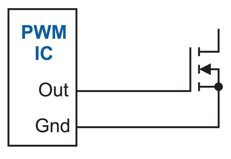
Figure 1: The power FET is driven directly from the output of the PWM controller.
The direct connection can be used when the control circuit shares the same ground reference as the power circuit, and power levels are relatively low.
Data sheets show that several amps can be provided from the PWM controller output, more than enough to drive low-power devices. However, a FET input is a large capacitance, and it’s usually not a good idea to try and use the full available current. It can lead to increased EMI due to rapid turn on and turn-off, excessive reverse recovery loss in rectifiers, and noise issues inside the PWM controller itself. Clock jitter, and sporadic interruptions in the normal operations can occur. [2].
It’s a good idea to limit the current from the PWM controller with the network shown in Fig. 2. Two resistors are used– one to control the turn-on time, and one to control the turn-off time. A diode is used to separate the two functions, but can be omitted in some cases if the timings are less critical.
We usually turn on the FET slowly when running a low-power converter. Don’t be afraid to experiment with the value of the resistor Ron. I’ve used values as low as 1 ohm, and as high as 1 kohm in designs. My rule of design is to increase the resistor while monitoring the switching waveforms and power dissipation in the FET. If the temperature starts to rise significantly, cut the value of the resistor in half. For a DCM flyback, it is surprising how slowly you can turn on the device without significant switching loss.
Turn off needs to be faster to provide rapid shut down in case of overcurrent conditions. Experiment with different values, don’t just use the value that might be shown in an application note. For more information on how fast you have to control the FET, refer to [3].
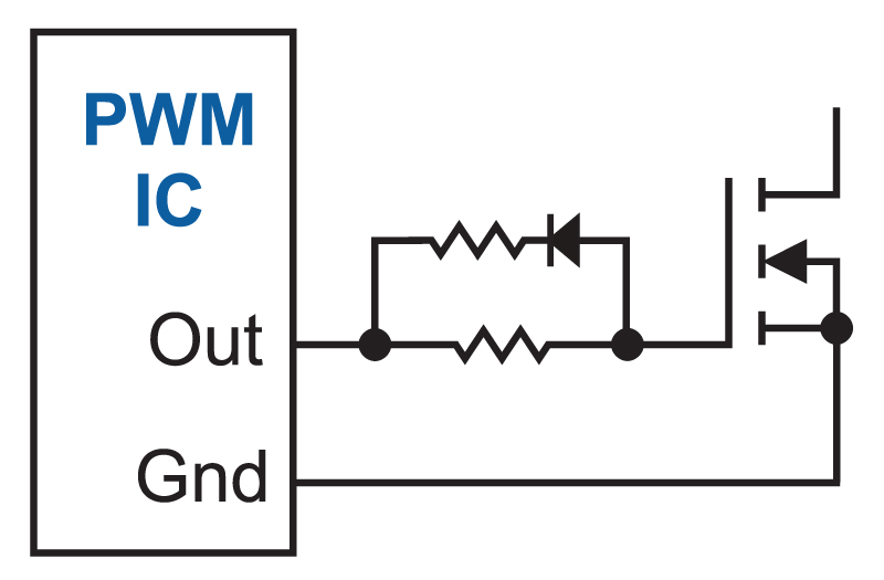
Figure 2: Slow-down resistors are used to control the turn-on and turn-off time of the power FET. We usually turn the device off faster than it is turned on in order to achieve fast current protection.
Dedicated Gate Drivers
As power levels rise, you will find the values of the gate resistors need to decrease to minimize switching loss. For higher power circuits, it is common industry practice to use a high-current driver chip. This prevents interference with the PWM controller, and also allows better layout of the PCB. There are many good drivers on the market, or you can even build your own high-current totem-pole driver if you want to raise performance while reducing cost.

Figure 3: For larger power devices, and higher power switching, it’s a good idea to use separate gate drive circuits to switch the devices rapidly. Gate resistors are still used, but are not shown here.
Transformer-Isolated Gate Drives
At higher power levels, we start to use topologies such as the two-switch forward converter, half-bridge converter, or full-bridge converter. All of these topologies require a floating switch to be driven.
There are silicon solutions to this problem. I would use these for low voltage applications, but not for off-line circuits. High-side integrated drivers remove too much control from the designer, and do not provide the same level of protection, isolation, immunity from transients, or common-mode noise rejection as a well-designed and implemented gate drive transformer.
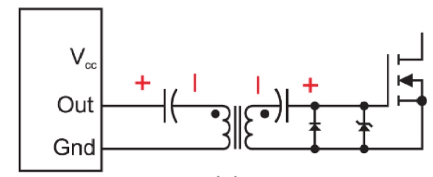
Fig. 4 shows the most rugged way to achieve a floating drive. The output of the drive chip couples through a dc-blocking capacitor to a small transformer (usually a toroid for high performance.) The secondary is connected directly to the gate of the FET, and any slow-down resistors should be placed in the primary of the transformer. Note the use of zeners on the gate for transient protection. Catch diodes are needed at the output of the driver, and should not be omitted even if initial tests show there is no problem with the reactive current in the transformer.
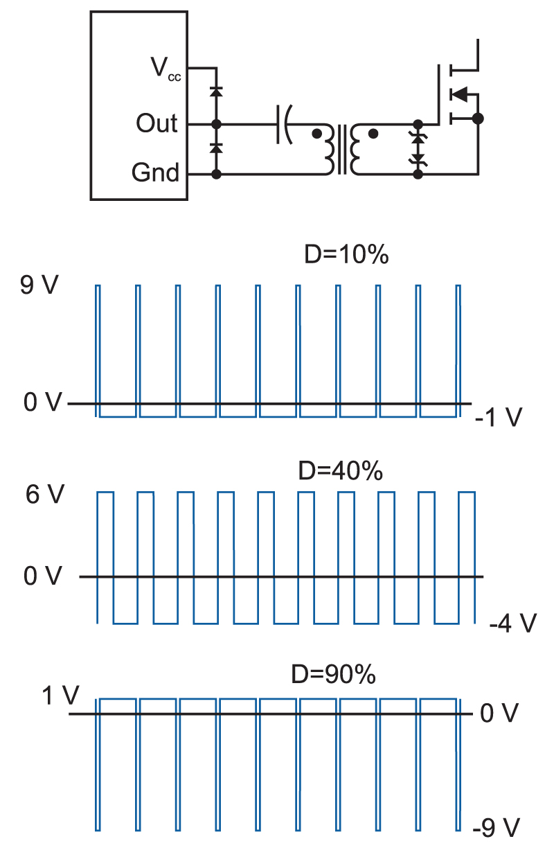
Figure 4: The most rugged scheme for isolated drives uses a gate drive transformer as shown. Catch diodes are needed for reactive current drives, and a dc blocking capacitor prevent saturation of the transformer. The capacitor causes a level shift in the output drive voltage, and this varies with duty cycle.
The circuit of Fig. 4 provides a secondary gate waveform with a negative value when the FET is off. This greatly enhances common-mode noise immunity, crucial for a bridge circuit. However, the negative waveform also has the disadvantage of reducing the voltage applied when the switch is on. At short duty cycles, the positive pulse is largest. At a 50% duty cycle, half the available gate voltage is lost, and at large duty cycles, there may not be enough voltage to properly turn the FET on. The transformer-coupled circuit is most effectively used with duty cycles from 0-50%. Fortunately, this is exactly what is needed for the forward, full- and half-bridge converters.
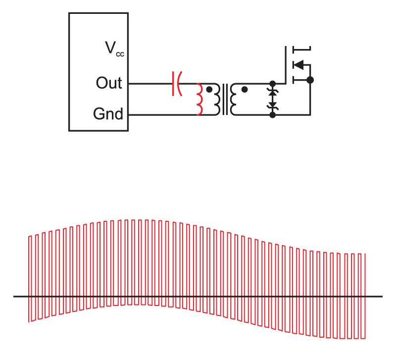
Figure 5: The dc coupling capacitor can ring with the magnetizing inductance of the gate drive transformer, usually during start-up and transients. This ringing should be properly damped to ensure safe operation.
Notice in Fig. 5 that the dc coupling capacitor can give rise to a low-frequency ringing superimposed on the gate drive waveform. The usual solution to this is to use a large value of capacitor which lowers the Q of the ringing waveform. Make sure you test all transient conditions, especially start up when the capacitor is initially discharged.
DC-Restorer Circuit – Watch Out!
Occasionally, you may run into a high-voltage circuit that needs an isolated gate drive close to 100%. In the past, the circuit of Fig. 6 has been recommended for this application.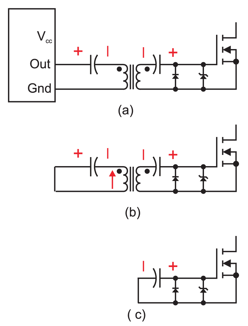
Figure 6: This dc-restorer circuit has been suggested for many years for circuits that require an isolated drive in excess of 50% duty cycle. This circuit can very often lead to failure when the power supply is turned off, and it is not recommended.
A diode and capacitor on the secondary restore the dc value of the gate drive, and allow the gate to be driven to duty cycles of up to 90% or more.
However, there is a serious flaw in this circuit, and it is not recommended for use without very careful analysis. The circuit works well during steady-state operation (a gate load resistor is recommended), but when the PWM controller shuts off, the dc blocking capacitor is connected across the gate drive transformer for an indefinite period. This can lead to saturation of the transformer, as shown in Fig. 6b. When the transformer saturates, the secondary is a short circuit, and the secondary capacitor can turn on the FET.
The saturation can be avoided with a gapped core, and smaller value of capacitor, but this will increase the reactive current needed from the gate driver, and may produce other problems.
Isolated Gate Drives for the Bridge Converters
The half- and full-bridge converters are isolated applications that need a very rugged drive scheme. During the switch off time, the opposite side of the bridge will turn on, impressing a high common-mode voltage to the off device.
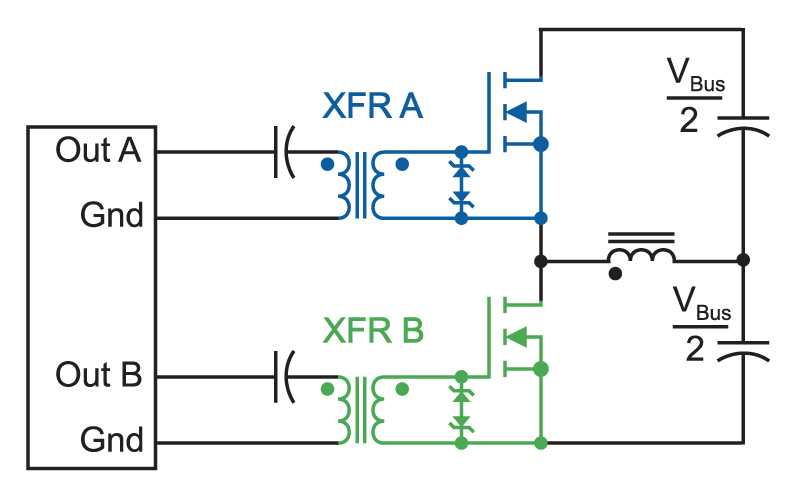
Figure 7: Two separate gate drive transformers are recommended for the half-bridge converter.
Fig. 7 shows the recommended scheme for a half-bridge converter. Two gate drive transformers should be used, don’t try to get away with just one transformer with a tri-state operation that you may see in some application notes.
The full-bridge converter, shown in Fig. 8, also needs two gate-drive transformers. Dual secondaries on each transformer are used to drive the pair of FETs on the diagonally-opposite legs of the bridge. For both types of bridges, the gate circuit should be thoroughly tested during start up transients where the highest peak currents are seen, and the negative drive of the gate is the smallest.
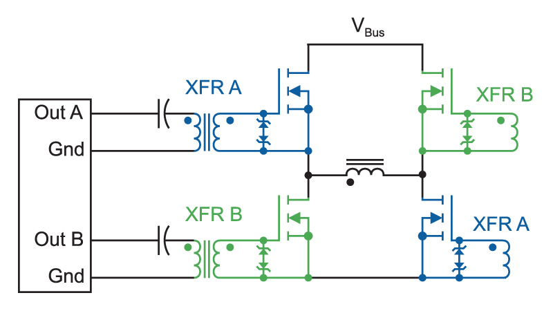
Figure 8: The full bridge converter also uses two transformers for rugged design. Two FETs are driven from two separate secondaries of each gate drive transformer.
The phase-shifted bridge in Fig. 9 also has two gate drive transformers, but notice the different arrangement. Each side of the bridge operates at a fixed 50% duty cycle, allowing the use of single gate drive transformer with dual secondaries of opposite polarities. This is one of the few circuits where the bipolar drive gate circuit can be used reliably. The only caveat is to be wary of the shut-down condition where ringing waveforms can turn on a device – there is no negative drive under this condition.
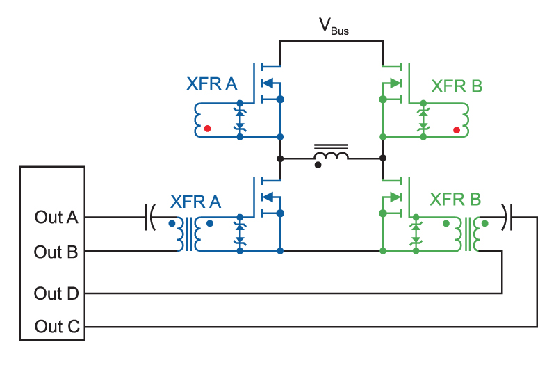
Figure 9: The phase-shifted full bridge uses a bi-directional transformer on each leg, Note the polarity of the secondaries.
Summary
Gate drive circuits are a crucial part of design. Make sure you use the right scheme, and don’t just blindly copy an application note. Gate drive transformers add a level of ruggedness to your design that cannot be achieved with silicon solutions. If you are designing at high power levels, they are an essential element. While you need to think through all the components in a gate drive, be careful not to overcomplicate the design. Additional active elements to supposedly speed up the device switching do not usually offer improvements in overall performance, but they do introduce new potential failure mechanisms. Keep your gate circuits as simple as possible.
Additional Reading
- Join our LinkedIn group titled “Power Supply Design Center”. Noncommercial site with over 7000 helpful members with lots of theoretical and practical experience.
- For power supply hands-on training, please sign up for our workshops.
- “Design and Application Guide for High Speed MOSFET Gate Drive Circuits”, Lazslo Balogh, Texas Instruments Application Note.
- “Six Reasons for Power Supply Instability”, Ray Ridley
- “Power Supply Stress Testing”, Ray Ridley
-
[005] High Frequency Power Inductor Design
Proximity Loss in Magnetics Windings
Exploring the use of custom versus off-the-shelf magnetics design. Standard parts are designed to a price point, and must be tested properly if you want to use them.
Power Supply Design Tips
In this article, we continue the theme of custom versus off-the-shelf magnetics design. The relatively simple output inductor of a forward converter is used as an example to show the issues and pitfalls involved in trying to use off-the-shelf inductor designs for high-frequency power supply applications.
Power Inductor Design
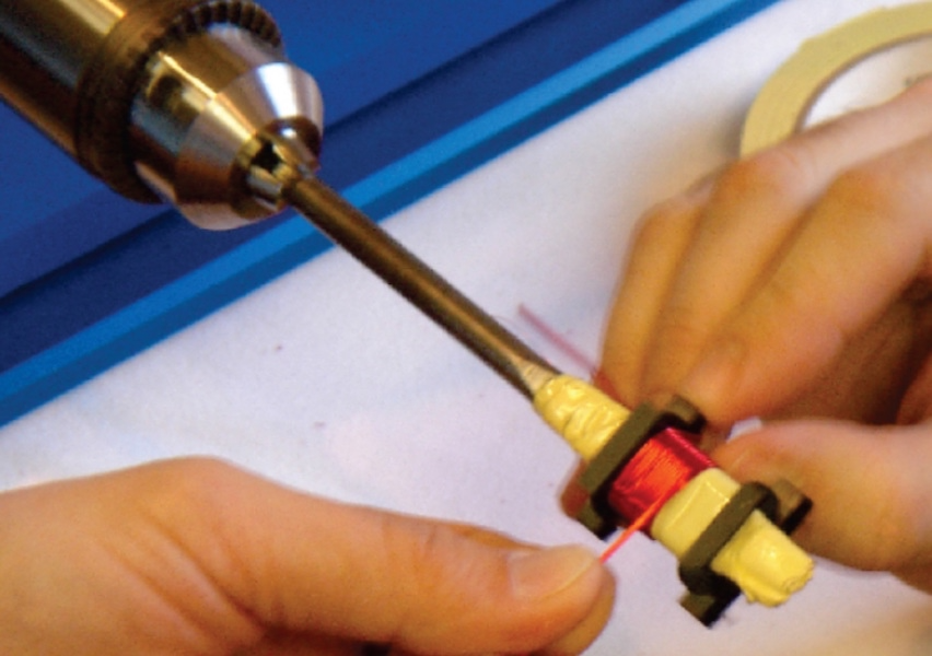
When I first started my career in power electronics, over 25 years ago, all magnetic components were custom designed and manufactured. In our current power supply design workshops, we dedicate an entire day to the theory and practice of making custom inductors for switching power supplies. Attendees at the course design, analyze, and build their own inductors and transformers in the lab.[1]
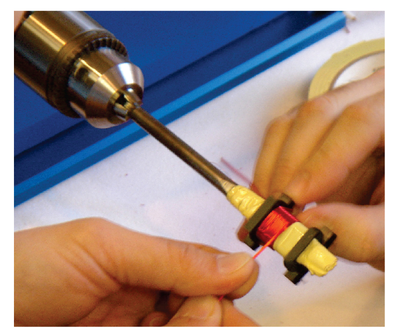
Figure 1: Building custom magnetics in our design workshop.
In the last few years, numerous companies have developed kits of standard parts aimed at the semiconductor companies to integrate into their designs. This proliferation of parts has recently led me to wonder if custom inductor design was becoming a skill belonging more to the past than the future.
Figure 2 shows two inductor designs, one developed in our workshop for a rugged 60-W converter, and the smaller low-cost, off-the-shelf part. You can see a significant size advantage of the standard component.
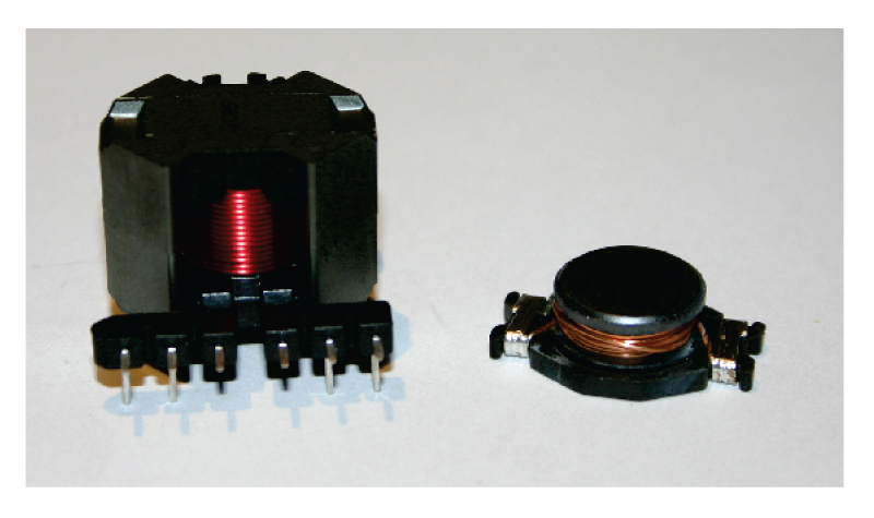
Figure 2: (a) 47 µH custom inductor and (b) off-the-shelf commodity component
The 47µH custom inductor was designed to operate continuously at 5 A, with plenty of margin for overcurrent situations.
The off-the-shelf inductor, also 47µH, had a single number assigned to it on the parts kit—a current rating of 5 A. Since the parts kit is aimed at the non-experienced power supply designer, it seems reasonable to assume that the inductor is suitable for a 5 A converter application
The parts are quite different in their design, as shown in Fig. 3. The custom-made inductor has a single-layer winding on an RM8 core, with a gapped center leg. The windings are a significant distance away from the center leg gap, essential to avoid proximity losses in the windings at high frequencies.
-
[007] Capacitors for Switching Power Supplies
The changing characteristics of the capacitors used in power supplies are examined. They are not as simple as most engineers assume.
Introduction
In several past articles, we have examined some of the complex characteristics of the power magnetics of a switching power supply. In this article, we examine another major passive component of the power supply—the capacitor. This is often a component that is viewed as a simple part that doesn’t require too much attention.
In this article, we examine another major passive component of the power supply—the capacitor. This is often a component that is viewed as a simple part that doesn’t require too much attention.
Power Supply Capacitors
Figure 1 shows the simple buck converter. Given modern integrated controllers, the design task of the engineer is apparently very simple—all we have to do is select and inductor and two capacitors, and the job is done. The choice of inductors can become very complex, and now we’ll see how capacitors can be troublesome, too.
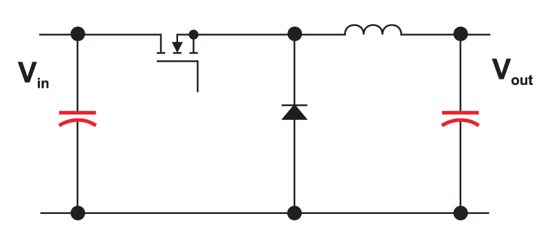
Figure 1: Buck converter with critical capacitor components. The output capacitor impedance determines the mid- and high-frequency response of the converter using either voltage-mode, current-mode, or any other form of control, including digital.
I’m often asked to perform worst-case analysis of switching power supply designs like this for companies. Step one of this process usually consists of the company sending me schematics, parts lists, and component data sheets. Before proceeding further, I always have to ask for working physical samples of the power supplies to test on the bench. To the alarm of people not familiar with power supplies, much of the worst-case analysis depends on measurements of existing designs, combined with documented datasheet variations which will shift the design.
Component data sheets are rarely adequate for properly characterizing parts, and a comprehensive analysis requires information either not readily available from manufacturers. Additional measurements are needed for magnetics, and additional measurements are needed for capacitors, too.
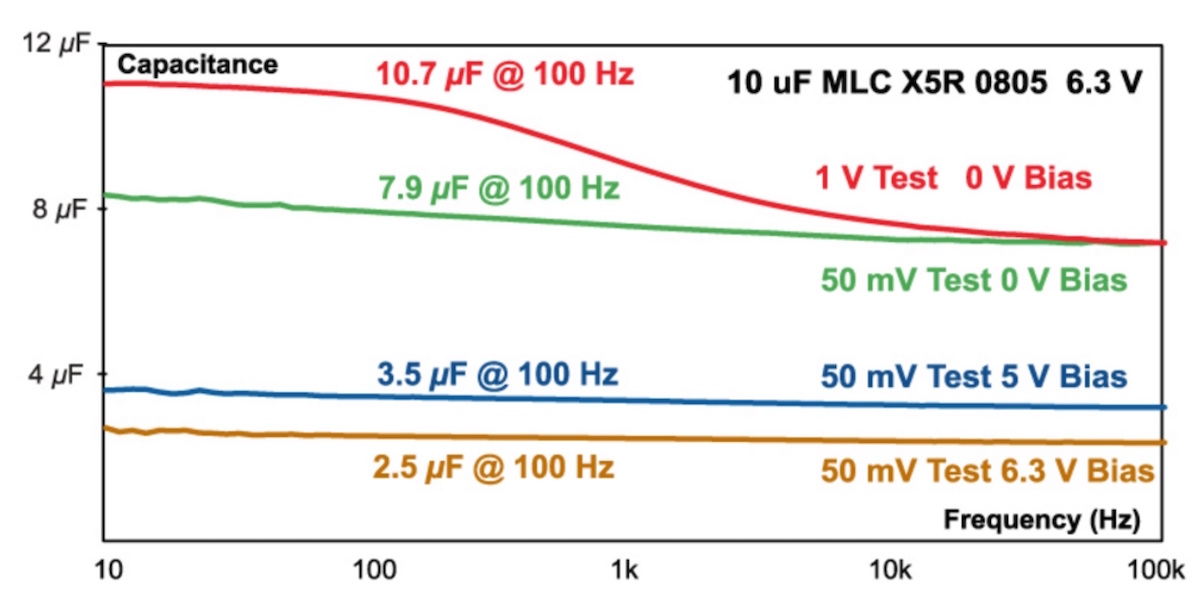
Low-Impedance Capacitor Measurement
A simple fixed RLC tester with a single measurement frequency is not adequate for characterizing capacitors for use in a modern switching power supply. The capacitors must be measured over a wide range of frequency to fully characterize their behavior.
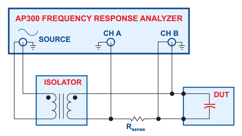
Figure 2: Measurement setup for low-impedance capacitors
Figure 2 shows how to make measurements of low-impedance capacitors with a frequency response analyzer [1]. Proper choice of sensing resistor, and proper RF layout of the test circuits will allow you to measure impedances as low as 1 mOhm with this test setup. While many component testers will only look at a single frequency, or a narrow range of frequencies, it is recommended that you sweep the frequency to see the impedance of the component under test from 10 Hz to at least 10 MHz.
-
[099] Modern Magnetics Design
This article gives an example of how profound proximity effects can be.
Introduction
In this article, Dr. Ridley discusses one of the most difficult aspects of magnetics design and analysis: winding proximity loss. Without understanding proximity loss, there is a roadblock to reducing the size of the magnetics components.
The Size of Modern Magnectics
In the last ten years, tremendous strides have been made in semiconductors to increase the performance of high-frequency power supplies. New wide-bandgap technologies, and new packaging techniques have led to unprecedented levels of power density and converter efficiency. The future for power conversion has never been so exciting.
However, one component has stubbornly continued to defy proportional miniaturization—the magnetics. Invented in 1831, the power transformer remains a larger component than anticipated, and it does not seem to follow any version of Moore’s Law.
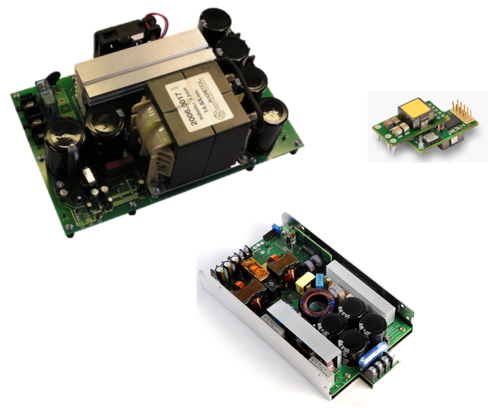
Figure 1: Modern Power Converter Size is Dominated by the Magnetic Components
Figure 1 shows modern power converters for different applications. A PFC circuit, LLC, and a point-of-load converter all feature prominent magnetics. In some cases, we find that the semiconductor devices no longer even need a heatsink and have disappeared from view underneath the circuit board. This emphasizes even more the need to work harder on the magnetics if we are to continue making progress with size reduction.
When starting a series of articles on magnetics design, it is customary to start at the beginning with design basics. Considerations of turns counts, saturation, core materials, and design optimization are usually at the forefront. You can learn more about some of these issues from ourmagnetics videos[1].
However, in this article, we are going to start with an advanced topic which causes severe problems for many designers. We will see in the example used in this article that conventional analysis of winding loss indicates that there will be just over 1 W of dissipation. However, detailed proximity loss analysis shows that, in reality, there isalmost 15 Wof power loss.
Forward Converter Design Example
Figure 2 shows an example forward converter running at 360 W. The converter runs at a switching frequency of 100 kHz. We will look at the detailed design of the transformer and show that it demonstrates excessive winding loss, despite initially good performance calculations.
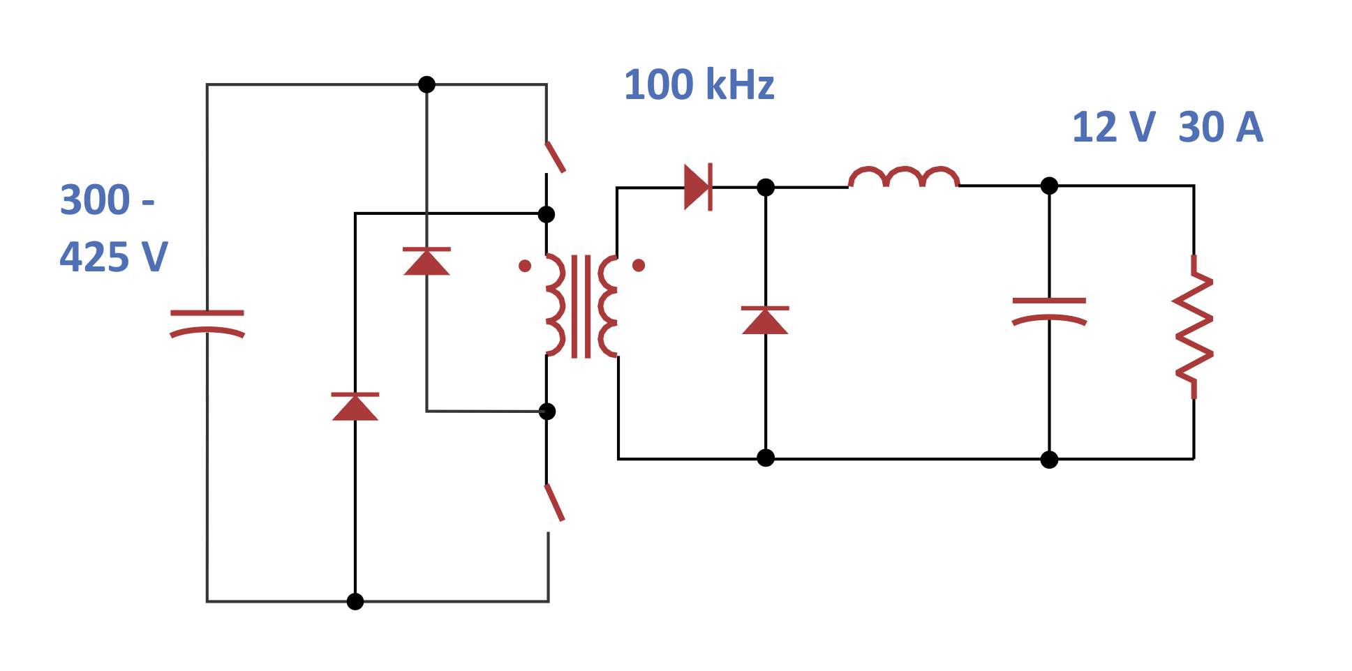
Figure 2: Two-Switch Forward Converter for 360 W Output