


Modeling
-
[002] Sepic Converter Analysis
The Sepic converter dc analysis is presented, showing why this is a popular converter. Beware of the ac characteristics though.
Introduction
In the last article, we talked about the simplest of all converters, the buck converter, and showed how its control transfer functions could be extraordinarily complex. In this issue, we’ll go to the other end of the spectrum, and look at a converter that is far more complex, yet is often used by engineers who are unaware of the difficulties they may be in for.
Call this article, if you like, part II of “Power Supplies are Supposed to be Easy!”
The Sepic Converter
The most basic converter that we looked at last month is the buck converter. It is so named because it always steps down, or bucks, the input voltage. The output of the converter is given by

Interchange the input and the output of the buck converter, and you get the second basic converter – the boost. The boost always steps up, hence its name. The output voltage is always higher than the input voltage, and is given by:

What if you have an application where you need to both step up and step down sometimes, depending on the input and output voltage? Well, you could use two cascaded converters, one a buck and one a boost. Unfortunately that needs two separate controllers and switches. (It’s actually a good solution in many cases, and should not be rejected out of hand.)
The buck-boost converter has the desired step up and step down functions

but the output is inverted. A flyback converter (isolated buck-boost) requires a transformer instead of just an inductor, adding to the complexity of the development.
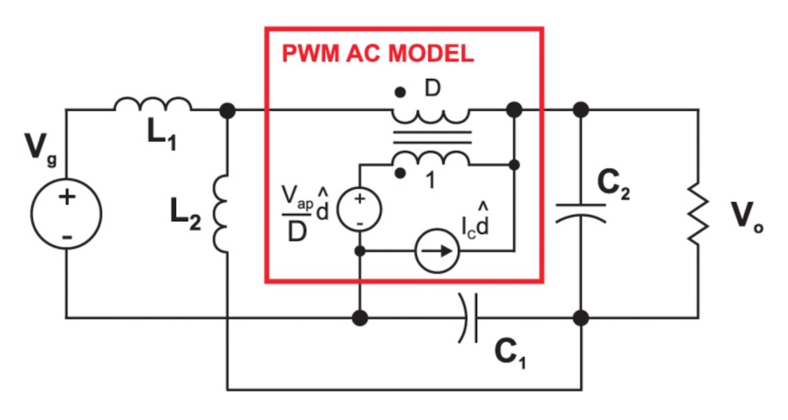
One converter that provides the needed input-to-output gain is the Sepic converter (single-ended primary inductor converter). This is shown in Fig. 1. It has become popular in recent years in battery-powered systems which must step up or down depending upon the charge level of the battery.
Figure 1: The Sepic converter can both step up and step down the input voltage, while maintaining the same polarity and the same ground reference for the input and output.
Fig. 2 shows the circuit when the power switch is turned on. The first inductor, L1, is charged from the input voltage source during this time. The second inductor takes energy from the first capacitor, and the output capacitor is left to provide the load current. The fact that both L1and L2 are disconnected from the load when the switch is on leads to complex control characteristics, as we will see later.
-
[004] HF Transformer Measurement and Modeling
How to measure and model high-frequency magnetics for switching power supplies. Essential steps for both custom-designed parts, or purchased components.
Power Supply Design Tips
This article points out some of the issues involved in designing, measuring, and modeling high-frequency magnetics for switching power supplies.
Despite efforts from some magnetics vendors to provide off-the-shelf components to power supply designers, almost all high-performance magnetics are custom. There are many deep and complex issues involved in the design of magnetics. I will try to cast some light on just a few of these issues.
Transformer Design Example
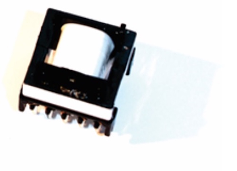
Figure 1 shows a simple 1:1 transformer. The transformer uses an ungapped EPC-25 core from TDK, made from PC-44 material. This transformer was designed for use in a 60 W forward converter with 36-60 V input and 12 V output.

Figure 1: A simple 1:1 transformer designed for a 100 kHz, 60 W forward converter.
Figure 2 shows the winding layout, with just a single layer of 18 turns for the primary winding, a layer of thin insulation tape, and a single layer of 18 turns for the secondary winding.
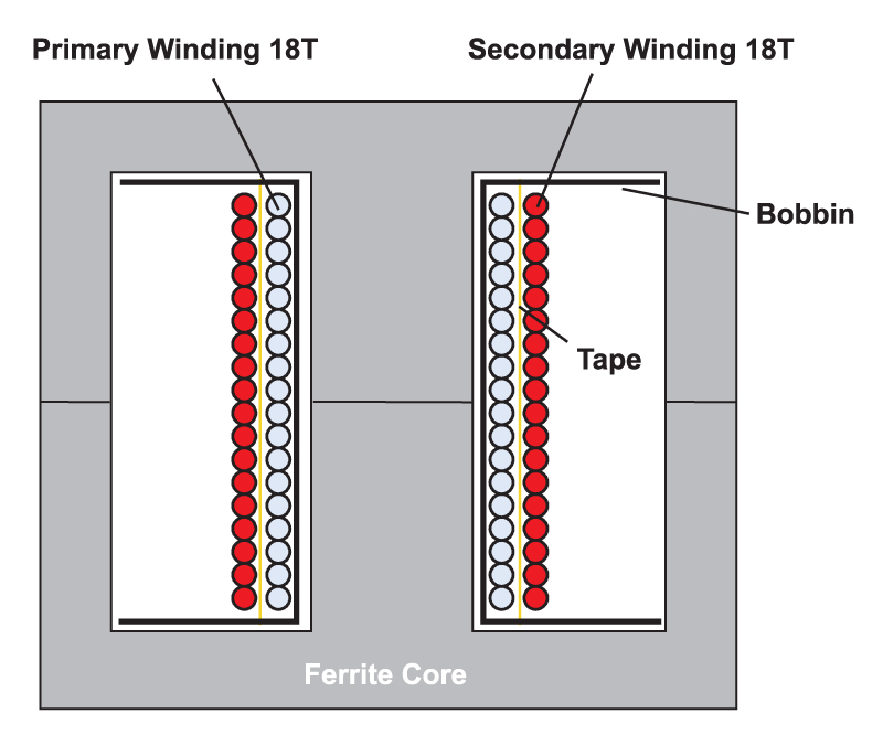
Figure 2: Winding layout of the transformer of Figure 1.
This is a very straightforward, easy-to-manufacture design of a two-winding transformer. However, as you will see below, the resulting circuit element created is anything but simple.
-
[099] Modern Magnetics Design
This article gives an example of how profound proximity effects can be.
Introduction
In this article, Dr. Ridley discusses one of the most difficult aspects of magnetics design and analysis: winding proximity loss. Without understanding proximity loss, there is a roadblock to reducing the size of the magnetics components.
The Size of Modern Magnectics
In the last ten years, tremendous strides have been made in semiconductors to increase the performance of high-frequency power supplies. New wide-bandgap technologies, and new packaging techniques have led to unprecedented levels of power density and converter efficiency. The future for power conversion has never been so exciting.
However, one component has stubbornly continued to defy proportional miniaturization—the magnetics. Invented in 1831, the power transformer remains a larger component than anticipated, and it does not seem to follow any version of Moore’s Law.
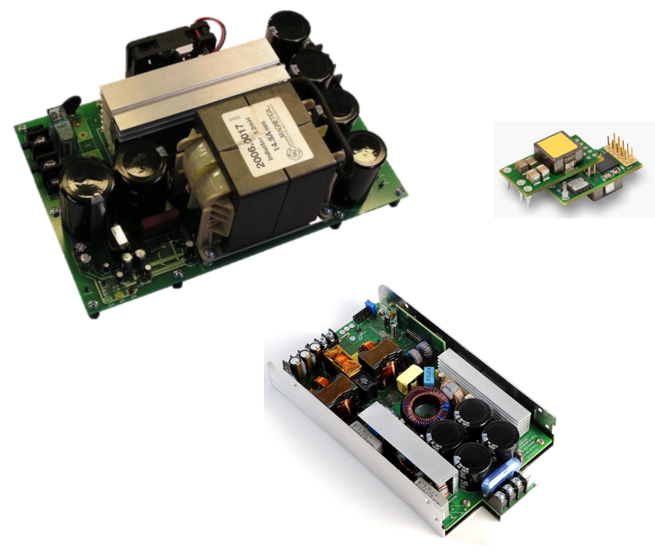
Figure 1: Modern Power Converter Size is Dominated by the Magnetic Components
Figure 1 shows modern power converters for different applications. A PFC circuit, LLC, and a point-of-load converter all feature prominent magnetics. In some cases, we find that the semiconductor devices no longer even need a heatsink and have disappeared from view underneath the circuit board. This emphasizes even more the need to work harder on the magnetics if we are to continue making progress with size reduction.
When starting a series of articles on magnetics design, it is customary to start at the beginning with design basics. Considerations of turns counts, saturation, core materials, and design optimization are usually at the forefront. You can learn more about some of these issues from ourmagnetics videos[1].
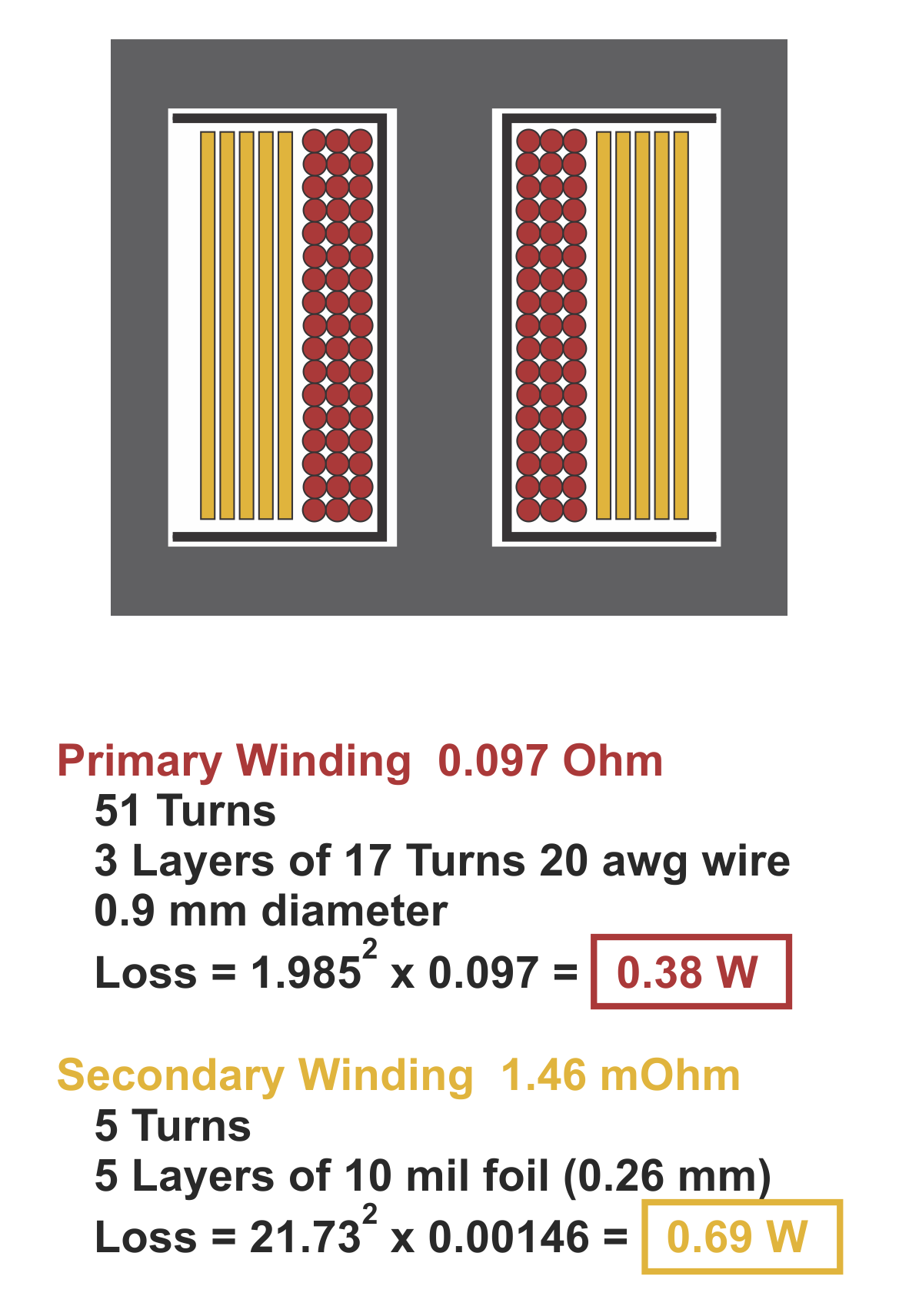
However, in this article, we are going to start with an advanced topic which causes severe problems for many designers. We will see in the example used in this article that conventional analysis of winding loss indicates that there will be just over 1 W of dissipation. However, detailed proximity loss analysis shows that, in reality, there isalmost 15 Wof power loss.
Forward Converter Design Example
Figure 2 shows an example forward converter running at 360 W. The converter runs at a switching frequency of 100 kHz. We will look at the detailed design of the transformer and show that it demonstrates excessive winding loss, despite initially good performance calculations.
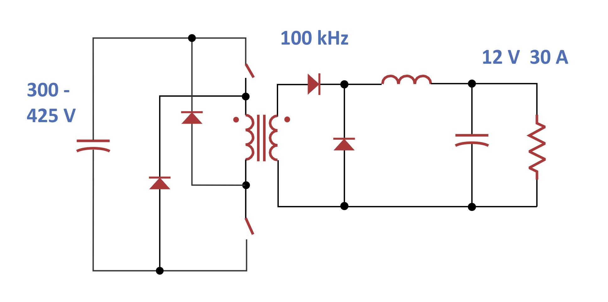
Figure 2: Two-Switch Forward Converter for 360 W Output