Even the simple buck converter can present very complex and changeable control characteristics when interacting with surrounding components and operating in different modes.
Introduction
This column is going to be devoted to the complex and intriguing issues that continue to make switching power supply design a challenging and time-consuming task. I hope to show you the need for proper diligence and engineering in designing the power supply, a crucial and often-misunderstood part of electronic systems.
Outside of the power supply design community, there is also an ever-present feeling that power supply design is easy, and not worthy of time and attention. Nothing could be further from the truth, and numerous product recalls in recent year related to power and heat issues are a testament to this fact.
There is no doubt that power supply design is a mature industry. Standard circuits are used in around the world, with flyback circuits, buck converters, and forward converters dominating the field. This has held stable for many years now, and as a result, there are strong efforts from semiconductor companies to integrate functions into advanced chips with more and more capability inside the chip, and fewer parts on the.
As the switching power supply functions become incorporated inside the chip, we often lose design flexibility, and access to crucial functions. I’ll talk in a future column about the parts that are being integrated, and why I personally prefer access to many of them with discrete designs. In this column, we’ll focus on just one of the functions that can be overlooked, the feedback control loop.
It has always been a specialty skill within power supply design to work on control. Too often, in the latest round of IC designs, the pretense is made that this is no longer a function that needs attention, and integration of the feedback loop eliminates the chance for proper system design.
Integration of discrete power circuits has happened before in this industry. Thirty years ago, when we didn’t yet have switchers to deal with, the industry was dominated by linear regulators. Sophisticated designs were generated by experienced engineers to optimize parameters such as the minimum dropout voltage, transient response time, thermal characteristics, efficiency, etc.
Designers were highly knowledgeable in transistor characteristics, thermal design, and feedback analysis. Since all regulators use error amplifiers to precisely set the output voltage, feedback analysis and measurement was part of the design procedure for an optimized system.
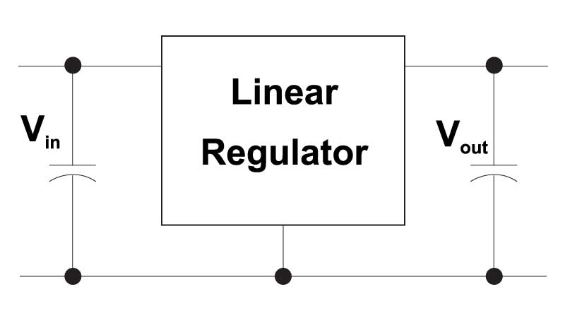
Later, standard solutions arrived in the industry, leading to integration of the linear regulator. Today, few of us ever consider building their own linear regulator since it has all been effectively integrated. In the process, access to the feedback loop has been lost, but no-one seems to be concerned about this. Why not? Well, the integration of the linear regulator went fairly smoothly, and there are three reasons for this – 1) predictability, 2) consistency with line and load variations, and 3) low noise.
Feedback for the linear regulator is quite straightforward. The small-signal model is just that of a current source feeding a capacitor and load resistor. The only variation in the design of a control loop for the system is in the impedance of the output capacitor. Apart from this, the system is predictable, and can easily be simulated, and modeled, with modeling results agreeing closely with measuremkkents.
Figure 1: Once designed with discrete components, the three-terminal linear regulator is now almost always fully integrated. There is no longer any access to the control loop.
Once the linear regulator was integrated, there was no opportunity left to change the controller, except for changing the output capacitor. And the output capacitor was really the only uncontrolled component. However, there is little stress placed upon this part – it is there just to stabilize the system, and provide energy during load transient.
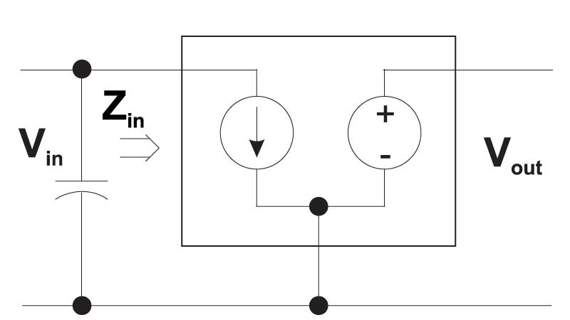
Once the linear regulator design is placed in the system, we can look at the characteristics of the regulator as the simple model shown in Figure 2. The input impedance of the linear regulator is a current source – regardless of changes in the input voltage, the current draw is fixed, equal to the output voltage divided by the load resistance. The output of the regulator model is just a voltage source.
Figure 2: As long as the linear regulator control loop is stable, the circuit model looks like a current source on the input (infinite impedance) and a voltage source on the output (very low impedance). Very little noise is introduced into the system.
Since the linear regulator does not generate any significant noise, we have no need to introduce any complex filtering on the system board. As a result, placement and integration of linear regulators on the board is a job that is almost trivial, and it does not require a power electronics designer to be involved (thermal issues notwithstanding – that’s often our responsibility, too.)
Does the future hold the same fate for the switching power supply? Will integration of the controller functions with power devices and auxiliary circuits render the switching power supply design a simple process?
Well, not quite so fast. As we’ll see below, even the simplest switching power supply has tremendous complexity of characteristics.
PWM Switching Regulators
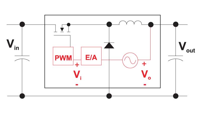
The most basic of all switching regulators is the buck converter, shown in Figure 3. It consists of just four power components, and a feedback loop, shown in red. It looks very simple, but as power designers have realized for decades, there is a lot of complexity to this system.
Figure 3: The apparently simple buck converter power stage consists of a switch, diode (or synchronous rectifier), inductor and capacitor. Feedback components are shown in red, with signal injection for transfer function measurements.
Once you are past the first step of turning on and off the semiconductor devices reliably and efficiently (not always an easy task, especially if you are dealing with synchronous rectifiers or isolated converters), you are left with a circuit that generates large amounts of noise, and one that needs a feedback loop designed around it for a stable regulated output.
I won’t talk about the turn on and turn off issues here – a topic for later. But first, let’s look at the control loop issues. The first step in dealing with control of any system is to properly understand its plant characteristics. For the buck converter of Figure 3, we are interested in how the power stage behaves, and we can measure a transfer function that shows this by looking at the ratio of Vo/Vi while injecting a swept sinusoidal source into the system. We can do this either in a simulation program, or on the hardware as described in reference [1].
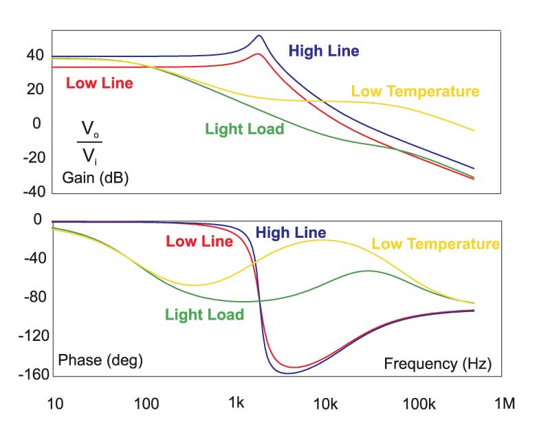
The blue and red curves of Figure 4 show the result of this for a buck converter operating at high and low line input. It’s basically just an LC filter characteristic with gain dependent on the input voltage.
Figure 4: This bode plot shows how much the control characteristics can change with variations is input line, output load, and temperature. At a typical crossover frequency of 10 kHz, the phase of the converter can vary by as much as 120 degrees, presenting a formidable challenge to the designer.
If the load is reduced enough, the converter will enter discontinuous mode, shown in the green curve (this does not happen with synchronous rectifiers). There’s a big change in the characteristics. Further change can occur if you have electrolytic capacitors in your system, and the temperature is reduced below freezing.
The resulting range of gain and phase curves with all these variations is much worse than a linear regulator loop would ever see. And this includes only the basic effects that can occur with switching regulators. Many more variations are with multiple output converters and noise issues [3].
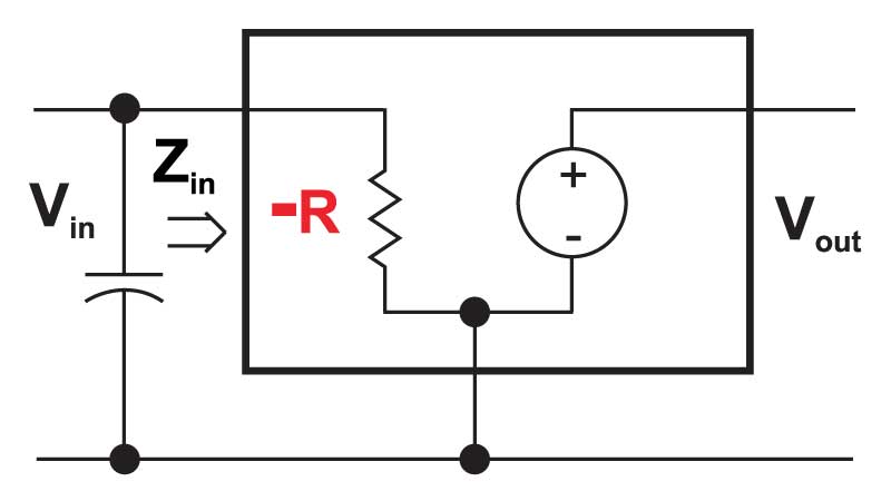
Now let’s take a look at what happens if you succeed in building an acceptable control loop with these variable characteristics. The closed-loop system has a simplified model that looks like that of Figure 5. The input impedance of the power supply looks like a negative resistor – quite different from the current source of the linear regulator. A negative resistor is a troublesome component in a system, frequently leading to oscillation.
Figure 5: Even if you manage to stabilize the buck converter by itself, once you put it in your system with proper filters to eliminate the noise from the converter, it can go unstable again. The negative input resistance can destabilize the passive components on the rest of your circuit board.
With input filters, it can actively excite the LC filters needed for the power supply under certain conditions [2], so great care must be paid to the choice of filter components.
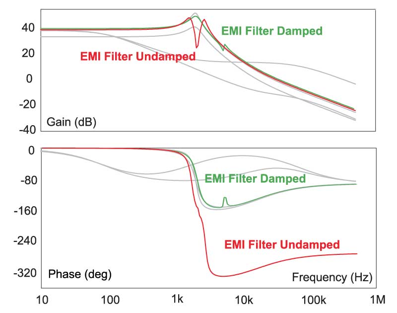
The effect of the filter can be seen in Figure 6. In the green curve, there is a small blip in the gain and phase of the power supply. The design is still OK, but it’s interacting with the filter. In the red curve, there is severe interaction, and the power stage suddenly has an additional 180 degrees phase delay in the control characteristic. This power supply will most likely be unstable.
Figure 6: Switching power supplies are noisy - LC filters must be added to the system to attenuate the noise. The green curve in this figure shows the effect control characteristics with a reasonably well-designed filter. The red curve shows what happens when the power supply will be unstable. Notice the additional 180 degrees phase delay where the input filter creates a pair of complex RHP zeros in the control loop. The total variation in phase at 10 kHz for the complete range of the power supply is now over 300 degrees!
There are many more situations that can be created, but hopefully the point has been made – switching power supplies will never be drop-in designs the way that linear regulators are. Proper engineering must be done to ensure that the switcher is incorporated into the system with the greatest of assurance they will be reliable.
Despite what you may read from companies trying to sell new power management products, the design of a switcher is still a complex task that needs proper engineering attention. Make sure you budget time and money accordingly, and bring the proper expertise into your project.
Additional Reading
- Join our LinkedIn group titled “Power Supply Design Center”. Noncommercial site with over 7000 helpful members with lots of theoretical and practical experience.
- For power supply hands-on training, please sign up for our workshops.
- Control function measurement techniques can be found at www.ridleyengineering.com
- Read about the effect of filters on switching regulators.
- For more reasons for converter instability.


