Control
-
[001] Complexities of Switching Power Design
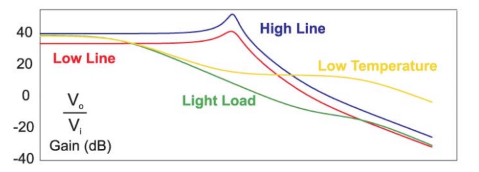
Even the simple buck converter can present very complex and changeable control characteristics when interacting with surrounding components and operating in different modes.
Introduction
This column is going to be devoted to the complex and intriguing issues that continue to make switching power supply design a challenging and time-consuming task. I hope to show you the need for proper diligence and engineering in designing the power supply, a crucial and often-misunderstood part of electronic systems.
Outside of the power supply design community, there is also an ever-present feeling that power supply design is easy, and not worthy of time and attention. Nothing could be further from the truth, and numerous product recalls in recent year related to power and heat issues are a testament to this fact.
There is no doubt that power supply design is a mature industry. Standard circuits are used in around the world, with flyback circuits, buck converters, and forward converters dominating the field. This has held stable for many years now, and as a result, there are strong efforts from semiconductor companies to integrate functions into advanced chips with more and more capability inside the chip, and fewer parts on the.
As the switching power supply functions become incorporated inside the chip, we often lose design flexibility, and access to crucial functions. I’ll talk in a future column about the parts that are being integrated, and why I personally prefer access to many of them with discrete designs. In this column, we’ll focus on just one of the functions that can be overlooked, the feedback control loop.
It has always been a specialty skill within power supply design to work on control. Too often, in the latest round of IC designs, the pretense is made that this is no longer a function that needs attention, and integration of the feedback loop eliminates the chance for proper system design.
Integration of discrete power circuits has happened before in this industry. Thirty years ago, when we didn’t yet have switchers to deal with, the industry was dominated by linear regulators. Sophisticated designs were generated by experienced engineers to optimize parameters such as the minimum dropout voltage, transient response time, thermal characteristics, efficiency, etc.
Designers were highly knowledgeable in transistor characteristics, thermal design, and feedback analysis. Since all regulators use error amplifiers to precisely set the output voltage, feedback analysis and measurement was part of the design procedure for an optimized system.
Later, standard solutions arrived in the industry, leading to integration of the linear regulator. Today, few of us ever consider building their own linear regulator since it has all been effectively integrated. In the process, access to the feedback loop has been lost, but no-one seems to be concerned about this. Why not? Well, the integration of the linear regulator went fairly smoothly, and there are three reasons for this – 1) predictability, 2) consistency with line and load variations, and 3) low noise.
Feedback for the linear regulator is quite straightforward. The small-signal model is just that of a current source feeding a capacitor and load resistor. The only variation in the design of a control loop for the system is in the impedance of the output capacitor. Apart from this, the system is predictable, and can easily be simulated, and modeled, with modeling results agreeing closely with measuremkkents.
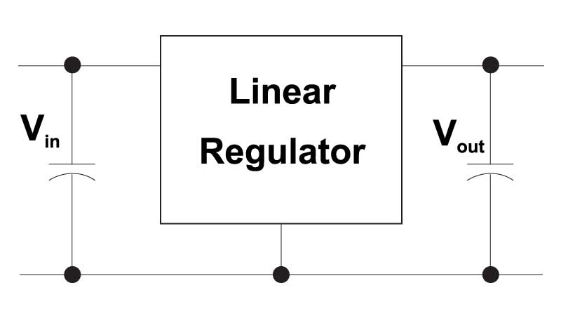
Figure 1: Once designed with discrete components, the three-terminal linear regulator is now almost always fully integrated. There is no longer any access to the control loop.
Once the linear regulator was integrated, there was no opportunity left to change the controller, except for changing the output capacitor. And the output capacitor was really the only uncontrolled component. However, there is little stress placed upon this part – it is there just to stabilize the system, and provide energy during load transient.
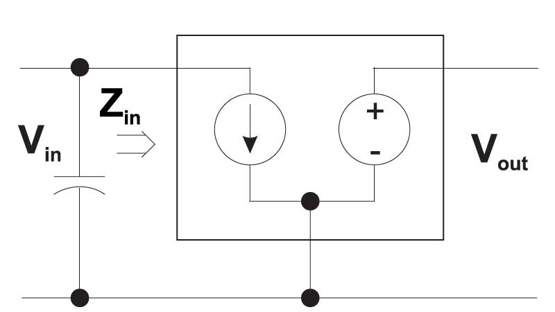
Once the linear regulator design is placed in the system, we can look at the characteristics of the regulator as the simple model shown in Figure 2. The input impedance of the linear regulator is a current source – regardless of changes in the input voltage, the current draw is fixed, equal to the output voltage divided by the load resistance. The output of the regulator model is just a voltage source.
Figure 2: As long as the linear regulator control loop is stable, the circuit model looks like a current source on the input (infinite impedance) and a voltage source on the output (very low impedance). Very little noise is introduced into the system.
Since the linear regulator does not generate any significant noise, we have no need to introduce any complex filtering on the system board. As a result, placement and integration of linear regulators on the board is a job that is almost trivial, and it does not require a power electronics designer to be involved (thermal issues notwithstanding – that’s often our responsibility, too.)
Does the future hold the same fate for the switching power supply? Will integration of the controller functions with power devices and auxiliary circuits render the switching power supply design a simple process?
Well, not quite so fast. As we’ll see below, even the simplest switching power supply has tremendous complexity of characteristics.
-
[002] Sepic Converter Analysis
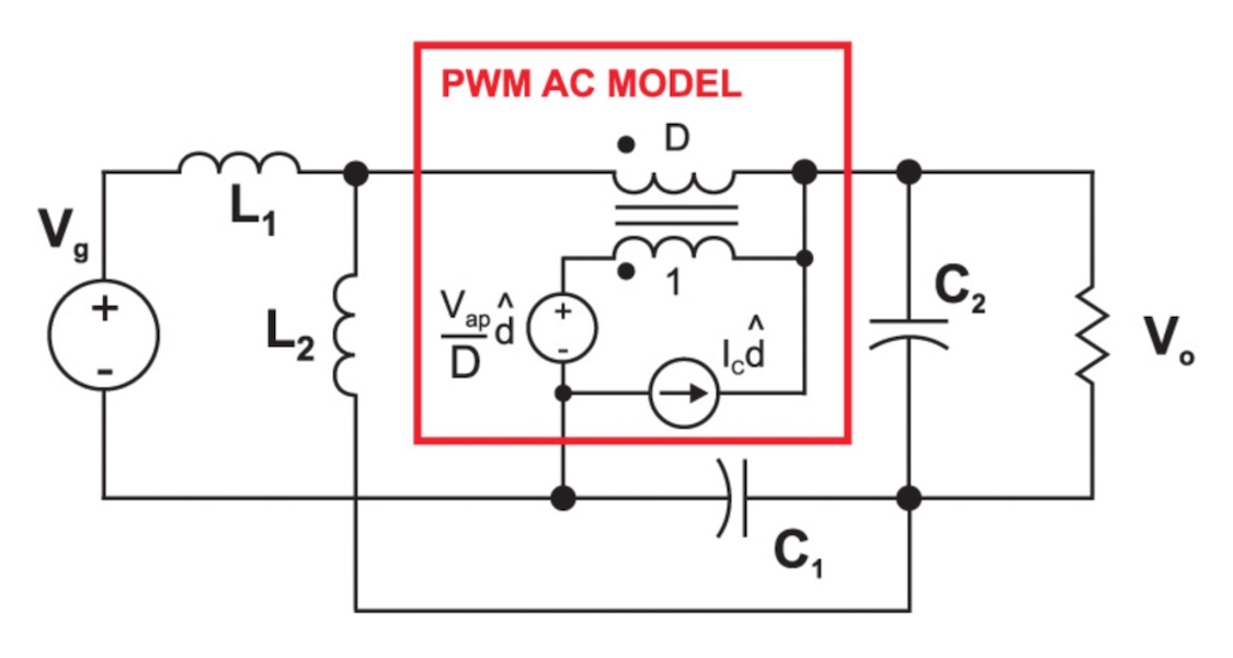
The Sepic converter dc analysis is presented, showing why this is a popular converter. Beware of the ac characteristics though.
Introduction
In the last article, we talked about the simplest of all converters, the buck converter, and showed how its control transfer functions could be extraordinarily complex. In this issue, we’ll go to the other end of the spectrum, and look at a converter that is far more complex, yet is often used by engineers who are unaware of the difficulties they may be in for.
Call this article, if you like, part II of “Power Supplies are Supposed to be Easy!”
The Sepic Converter
The most basic converter that we looked at last month is the buck converter. It is so named because it always steps down, or bucks, the input voltage. The output of the converter is given by

Interchange the input and the output of the buck converter, and you get the second basic converter – the boost. The boost always steps up, hence its name. The output voltage is always higher than the input voltage, and is given by:

What if you have an application where you need to both step up and step down sometimes, depending on the input and output voltage? Well, you could use two cascaded converters, one a buck and one a boost. Unfortunately that needs two separate controllers and switches. (It’s actually a good solution in many cases, and should not be rejected out of hand.)
The buck-boost converter has the desired step up and step down functions

but the output is inverted. A flyback converter (isolated buck-boost) requires a transformer instead of just an inductor, adding to the complexity of the development.
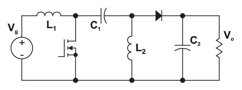
One converter that provides the needed input-to-output gain is the Sepic converter (single-ended primary inductor converter). This is shown in Fig. 1. It has become popular in recent years in battery-powered systems which must step up or down depending upon the charge level of the battery.
Figure 1: The Sepic converter can both step up and step down the input voltage, while maintaining the same polarity and the same ground reference for the input and output.
Fig. 2 shows the circuit when the power switch is turned on. The first inductor, L1, is charged from the input voltage source during this time. The second inductor takes energy from the first capacitor, and the output capacitor is left to provide the load current. The fact that both L1and L2 are disconnected from the load when the switch is on leads to complex control characteristics, as we will see later.
-
[006] The Digital Power Supply Revolution

Digital power is all the rage now, but don't expect it to shorten your design time, or to eliminate the need for complete optimization of the analog parts of the power supply.
Introduction
At the recent Applied Power Electronics Conference, digital power supplies were featured everywhere, in papers, seminars, and poster sessions. Applications were widespread, in VRMs, power factor correction circuits, inverters, and dc-dc converters.
It’s easy to start feeling overwhelmed with all this information on digital applications. And, in reading the material, to feel like you are perhaps missing the boat with your simple analog solutions. In this article, I’ll examine some of the issues and misconceptions about digital control.
Digital Control is New?
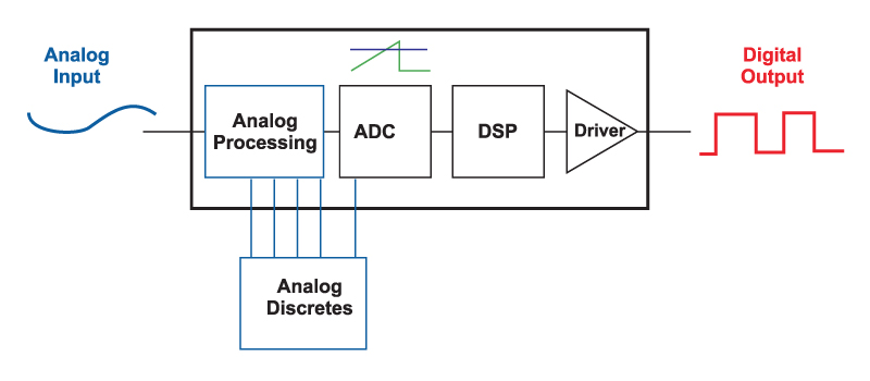
Figure 1 shows the block diagram of a digital controller. At the input side, an a/d converter samples an analog waveform of the power supply, and converts it to a digital value. The analog waveform may be the output voltage, or some pre-processed waveform where it has already been compared to a reference.
Sampling is done carefully, in an effort to avoid switching noise from affecting the results, and this simple sampling process can be quite complex, especially if there are multiple converters operating together in a system.
Figure 1: Block diagram of Digital Controller
The resulting digital signal then enters the processor of the digital controller, which sends the gate drive to the system. The driver circuitry may or may not be included in the controller, and this was discussed in the December 2006 issue of this magazine.
Much of the focus in recent years has been concentrated on solving the issues of the resolution of the digital output pulse. Numerous researchers have come up with solutions, including delay gates, to provide resolution beyond the clock frequency of the digital controller. This is important to avoid numerical oscillation.
Now let’s look at the so-called analog controller—yesterday’s technology if you listen to all the digital papers. Figure 2 shows a typical controller. The output voltage of a converter is processed with an analog amplifier, and discrete analog parts are used to compensate the feedback. The output of the error amplifier then is compared to a ramp with a comparator. The ramp also forms the clock of the converter.
Figure 2: Block diagram of “Analog” Controller
The ramp-reference circuit is nothing more than a simple A-D converter, directly generating a digital waveform, and setting the width of the pulse at the output of the controller. If you look at the input and output waveforms of Figure 1 and Figure 2, one thing should be immediately obvious: the analog controller that we have used for over 20 years in this industry is, in fact, a digital controller!
It has all the features required—and ADC, digital processing circuitry, and digital output. It is also an incredibly elegant solution to the digital controller problem. The clock frequency does not need to be any higher than the desired switching frequency of the power supply, and yet the output digital pulse has infinite resolution. This is something the new digital controllers are still struggling to achieve.
It is very important to recognize that the controllers we’ve always used are digital controllers. It stops us from worrying about whether we are using the latest in technology—analog or digital—when in fact they are both digital with different implementations. And it moves us forward to consider what the real difference is between the old and new, and whether you need it.
The core difference is that the new controllers are programmed with software, whereas the old controllers are hard wired, and not as flexible. As we’ll see in this article, the capability to reprogram may not be as important as claimed for your converter.
-
[023] Frequency Response Measurement Part I: Wide Band of Frequencies
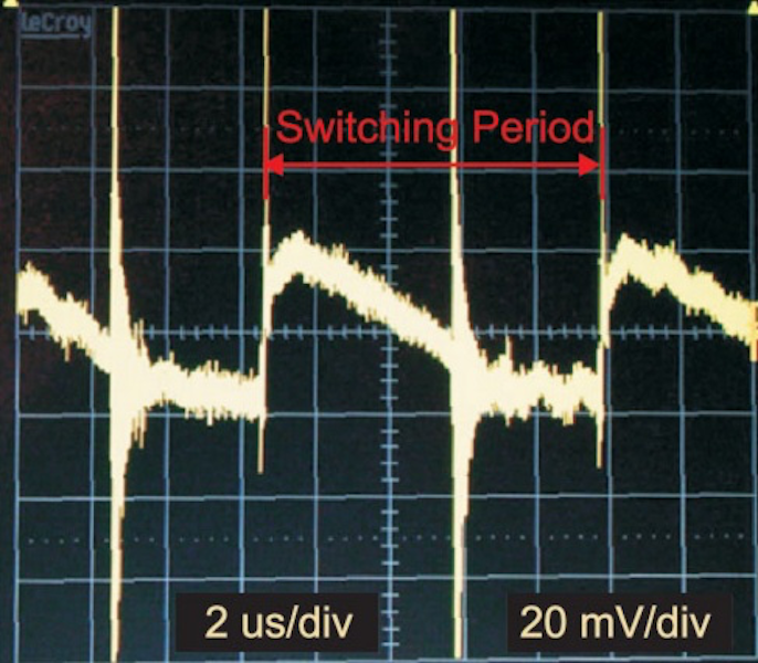
The needed frequency range of power supply design and analysis is explored.
Introduction
In this article, Dr. Ridley starts a series of three articles on switching power supply frequency response. The first article introduces the frequency ranges of interest in a switching power supply, and some of the difficulties of frequency response analysis.
Switching Power Supplies – Ultra Wide Band Circuits
Switching power supplies have a reputation for being difficult circuits to design, troubleshoot, and manufacture. Some of the reasons for this have been covered in past articles in Power Systems Design Europe [1]. There is another fundamental issue encountered with power supplies that makes them a special class of electronics: they generate an extraordinarily wide range of frequencies.
Sometimes it is easy to point at RF fields and be in awe at the extremely high frequencies encountered, in the multi-GHz range. Anyone who has worked in these fields is familiar with the critical parameters of circuit layouts, microwave circuit elements, matching networks, and other specialties. The 100 kHz switching power supply seems relatively easy by comparison.
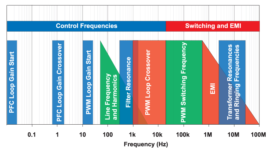
A major challenge of the switching power supply design is encountered in the extreme range of frequencies that must be considered. Figure 1 shows the typical frequency bands for a switching power supply.
There are two significantly separate regions of Figure 1. The first region concerns the frequencies up to half of the switching frequency. These are the relevant control frequencies of the converter, where the control loop responds to changes in the system such as changing loads, or changing input voltages.
The second region is from the switching frequency and up. For these frequencies, the power supply is a noise or EMI generator. The power supply is not expected to respond to a control stimulus in these frequency ranges, and the job of the power supply designer is to suppress and manage the high frequency noise components.
Control Frequencies
Control Frequencies of a power supply can extend down as low as 0.01 Hz, and as high as several hundred kHz, depending on the switching frequency (typically in the range of 20 kHz to 2 MHz.)
Many power supplies are now designed with two stages of power conversion – a switching power factor correction circuit (PFC) which shapes the AC input current waveform, and a switching DC-DC power supply which isolates and regulates the output from the input source power.
The function of the PFC circuit is to make the input of the system look like just a resistive load, even though there are large bulk capacitors to be charged at the input. To achieve this, the primary purpose of the PFC circuit is to shape the input current into a rectified AC waveform. (A feedback loop from the output capacitor after this circuit is used to set the average current level during the AC line cycle.)
If the input current waveform is to have low distortion, the feedback signal setting the current level must remain essentially constant during a single line cycle. This means that the loop around the PFC circuit must be slow – with a bandwidth of perhaps no more than 1 Hz. This PFC circuit requirement sets the first two bands of Figure 1 – the PFC loop gain is typically measured in the range from 0.01 Hz to 10 Hz.
10 Hz is typically where a loop gain Bode plot is initiated for the switching power supply. This frequency is chosen since it is below the significant noise frequency caused by the AC input line. The AC input line generates noise at 50 or 60 Hz with a single-diode rectifier, and at 100 or 120 Hz with a bridge rectifier. The control of the power supply is expected to respond to prevent the line-frequency harmonics from appearing on the output of the power supply.
The resonance of the LC filter of a switching power supply is typically around 100 times lower than the selected switching frequency. For a 100 kHz power supply, a resonance of 1 kHz is typical.
The loop gain of the converter can be as high as about 1/10th the switching frequency [2], and as low as perhaps 100 Hz. While the actual crossover itself is not a design objective, raising the crossover frequency is usually a method to improve performance without making significant changes to power components. Loop gain measurements are continued above the crossover frequency and up to the switching frequency, to verify the gain margin of the system.


