Magnetics
-
[001] Complexities of Switching Power Design
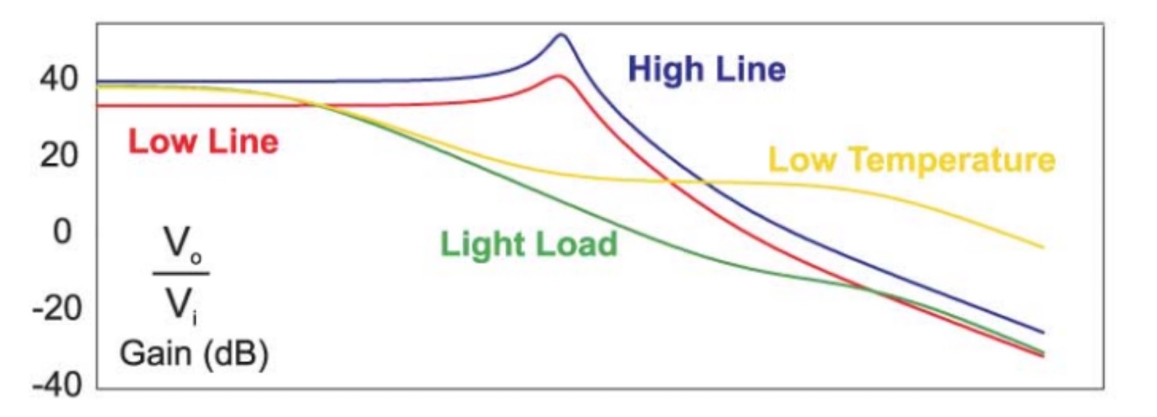
Even the simple buck converter can present very complex and changeable control characteristics when interacting with surrounding components and operating in different modes.
Introduction
This column is going to be devoted to the complex and intriguing issues that continue to make switching power supply design a challenging and time-consuming task. I hope to show you the need for proper diligence and engineering in designing the power supply, a crucial and often-misunderstood part of electronic systems.
Outside of the power supply design community, there is also an ever-present feeling that power supply design is easy, and not worthy of time and attention. Nothing could be further from the truth, and numerous product recalls in recent year related to power and heat issues are a testament to this fact.
There is no doubt that power supply design is a mature industry. Standard circuits are used in around the world, with flyback circuits, buck converters, and forward converters dominating the field. This has held stable for many years now, and as a result, there are strong efforts from semiconductor companies to integrate functions into advanced chips with more and more capability inside the chip, and fewer parts on the.
As the switching power supply functions become incorporated inside the chip, we often lose design flexibility, and access to crucial functions. I’ll talk in a future column about the parts that are being integrated, and why I personally prefer access to many of them with discrete designs. In this column, we’ll focus on just one of the functions that can be overlooked, the feedback control loop.
It has always been a specialty skill within power supply design to work on control. Too often, in the latest round of IC designs, the pretense is made that this is no longer a function that needs attention, and integration of the feedback loop eliminates the chance for proper system design.
Integration of discrete power circuits has happened before in this industry. Thirty years ago, when we didn’t yet have switchers to deal with, the industry was dominated by linear regulators. Sophisticated designs were generated by experienced engineers to optimize parameters such as the minimum dropout voltage, transient response time, thermal characteristics, efficiency, etc.
Designers were highly knowledgeable in transistor characteristics, thermal design, and feedback analysis. Since all regulators use error amplifiers to precisely set the output voltage, feedback analysis and measurement was part of the design procedure for an optimized system.
Later, standard solutions arrived in the industry, leading to integration of the linear regulator. Today, few of us ever consider building their own linear regulator since it has all been effectively integrated. In the process, access to the feedback loop has been lost, but no-one seems to be concerned about this. Why not? Well, the integration of the linear regulator went fairly smoothly, and there are three reasons for this – 1) predictability, 2) consistency with line and load variations, and 3) low noise.
Feedback for the linear regulator is quite straightforward. The small-signal model is just that of a current source feeding a capacitor and load resistor. The only variation in the design of a control loop for the system is in the impedance of the output capacitor. Apart from this, the system is predictable, and can easily be simulated, and modeled, with modeling results agreeing closely with measuremkkents.
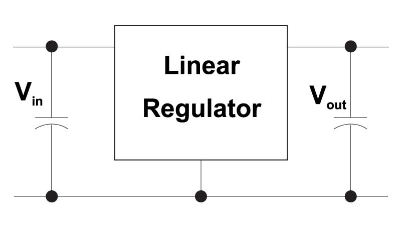
Figure 1: Once designed with discrete components, the three-terminal linear regulator is now almost always fully integrated. There is no longer any access to the control loop.
Once the linear regulator was integrated, there was no opportunity left to change the controller, except for changing the output capacitor. And the output capacitor was really the only uncontrolled component. However, there is little stress placed upon this part – it is there just to stabilize the system, and provide energy during load transient.
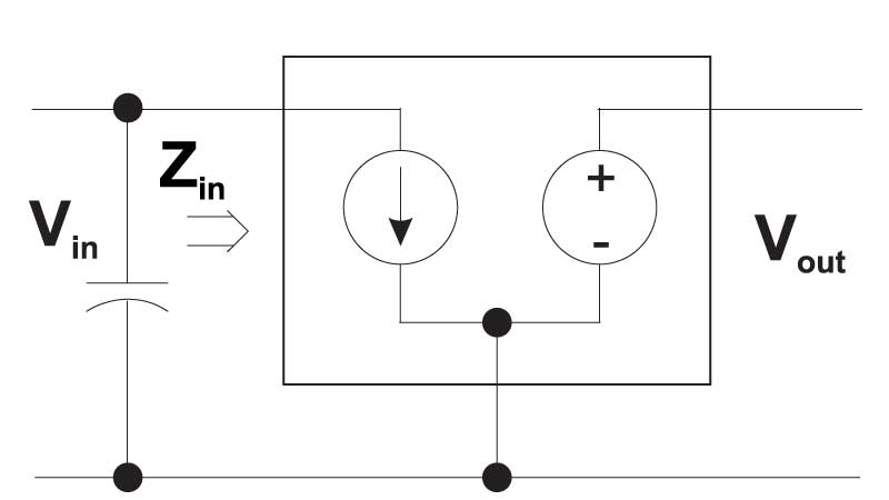
Once the linear regulator design is placed in the system, we can look at the characteristics of the regulator as the simple model shown in Figure 2. The input impedance of the linear regulator is a current source – regardless of changes in the input voltage, the current draw is fixed, equal to the output voltage divided by the load resistance. The output of the regulator model is just a voltage source.
Figure 2: As long as the linear regulator control loop is stable, the circuit model looks like a current source on the input (infinite impedance) and a voltage source on the output (very low impedance). Very little noise is introduced into the system.
Since the linear regulator does not generate any significant noise, we have no need to introduce any complex filtering on the system board. As a result, placement and integration of linear regulators on the board is a job that is almost trivial, and it does not require a power electronics designer to be involved (thermal issues notwithstanding – that’s often our responsibility, too.)
Does the future hold the same fate for the switching power supply? Will integration of the controller functions with power devices and auxiliary circuits render the switching power supply design a simple process?
Well, not quite so fast. As we’ll see below, even the simplest switching power supply has tremendous complexity of characteristics.
-
[004] HF Transformer Measurement and Modeling
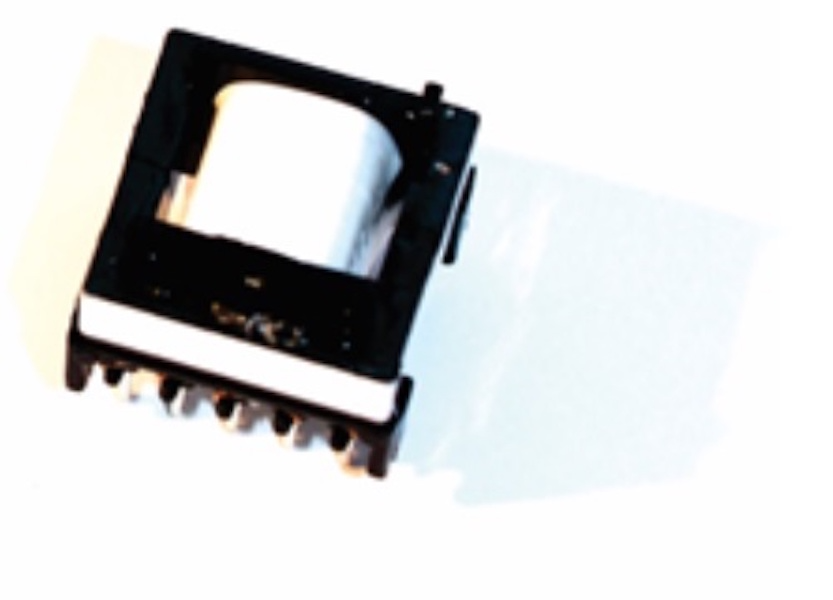
How to measure and model high-frequency magnetics for switching power supplies. Essential steps for both custom-designed parts, or purchased components.
Power Supply Design Tips
This article points out some of the issues involved in designing, measuring, and modeling high-frequency magnetics for switching power supplies.
Despite efforts from some magnetics vendors to provide off-the-shelf components to power supply designers, almost all high-performance magnetics are custom. There are many deep and complex issues involved in the design of magnetics. I will try to cast some light on just a few of these issues.
Transformer Design Example
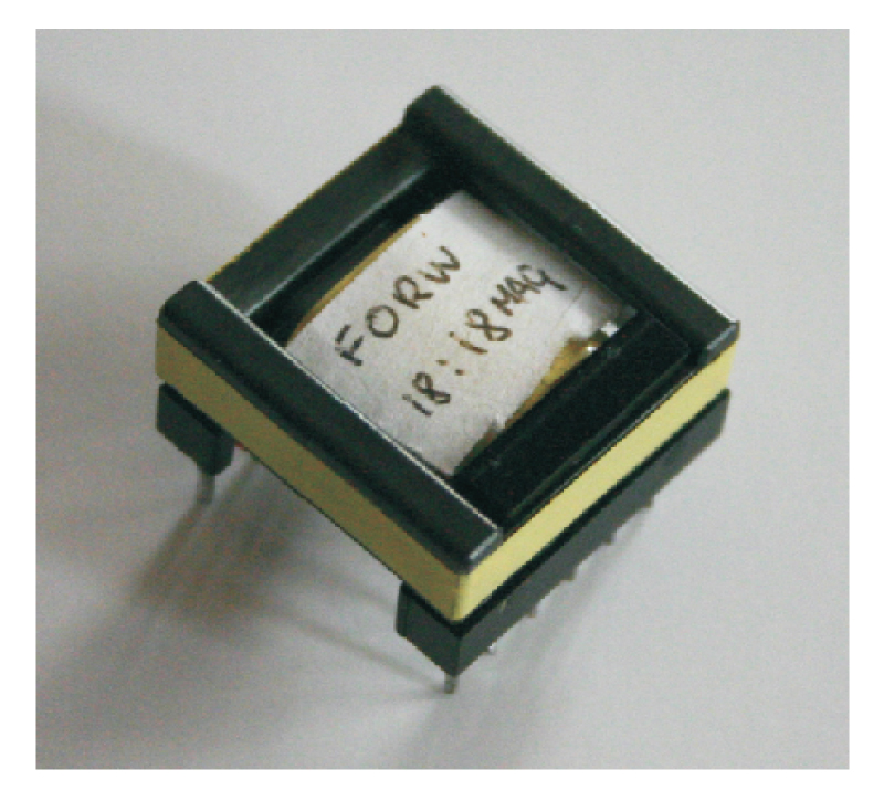
Figure 1 shows a simple 1:1 transformer. The transformer uses an ungapped EPC-25 core from TDK, made from PC-44 material. This transformer was designed for use in a 60 W forward converter with 36-60 V input and 12 V output.
Figure 1: A simple 1:1 transformer designed for a 100 kHz, 60 W forward converter.
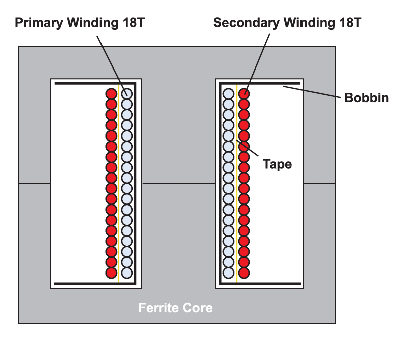
Figure 2 shows the winding layout, with just a single layer of 18 turns for the primary winding, a layer of thin insulation tape, and a single layer of 18 turns for the secondary winding.
Figure 2: Winding layout of the transformer of Figure 1.
This is a very straightforward, easy-to-manufacture design of a two-winding transformer. However, as you will see below, the resulting circuit element created is anything but simple.
-
[005] High Frequency Power Inductor Design

Proximity Loss in Magnetics Windings
Exploring the use of custom versus off-the-shelf magnetics design. Standard parts are designed to a price point, and must be tested properly if you want to use them.
Power Supply Design Tips
In this article, we continue the theme of custom versus off-the-shelf magnetics design. The relatively simple output inductor of a forward converter is used as an example to show the issues and pitfalls involved in trying to use off-the-shelf inductor designs for high-frequency power supply applications.
Power Inductor Design
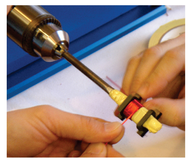
When I first started my career in power electronics, over 25 years ago, all magnetic components were custom designed and manufactured. In our current power supply design workshops, we dedicate an entire day to the theory and practice of making custom inductors for switching power supplies. Attendees at the course design, analyze, and build their own inductors and transformers in the lab.[1]
Figure 1: Building custom magnetics in our design workshop.
In the last few years, numerous companies have developed kits of standard parts aimed at the semiconductor companies to integrate into their designs. This proliferation of parts has recently led me to wonder if custom inductor design was becoming a skill belonging more to the past than the future.
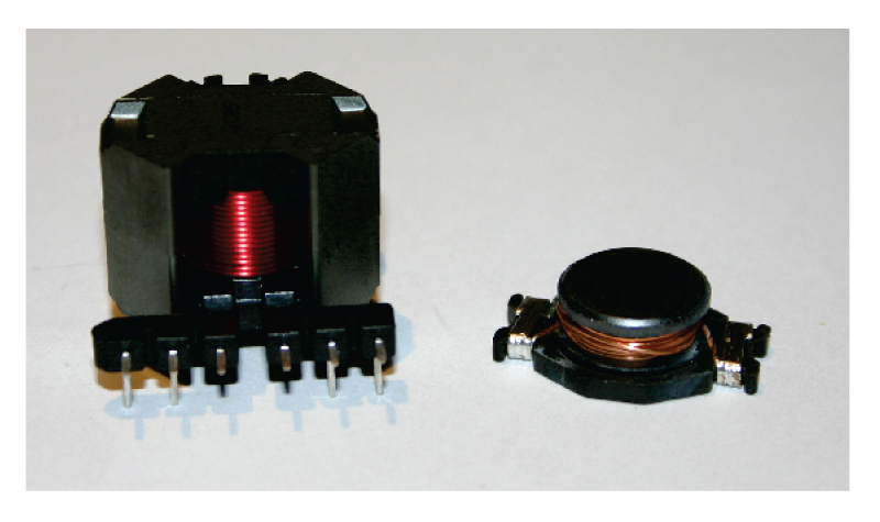
Figure 2 shows two inductor designs, one developed in our workshop for a rugged 60-W converter, and the smaller low-cost, off-the-shelf part. You can see a significant size advantage of the standard component.
Figure 2: (a) 47 µH custom inductor and (b) off-the-shelf commodity component
The 47µH custom inductor was designed to operate continuously at 5 A, with plenty of margin for overcurrent situations.
The off-the-shelf inductor, also 47µH, had a single number assigned to it on the parts kit—a current rating of 5 A. Since the parts kit is aimed at the non-experienced power supply designer, it seems reasonable to assume that the inductor is suitable for a 5 A converter application
The parts are quite different in their design, as shown in Fig. 3. The custom-made inductor has a single-layer winding on an RM8 core, with a gapped center leg. The windings are a significant distance away from the center leg gap, essential to avoid proximity losses in the windings at high frequencies.
-
[099] Modern Magnetics Design
This article gives an example of how profound proximity effects can be.
Introduction
In this article, Dr. Ridley discusses one of the most difficult aspects of magnetics design and analysis: winding proximity loss. Without understanding proximity loss, there is a roadblock to reducing the size of the magnetics components.
The Size of Modern Magnectics
In the last ten years, tremendous strides have been made in semiconductors to increase the performance of high-frequency power supplies. New wide-bandgap technologies, and new packaging techniques have led to unprecedented levels of power density and converter efficiency. The future for power conversion has never been so exciting.
However, one component has stubbornly continued to defy proportional miniaturization—the magnetics. Invented in 1831, the power transformer remains a larger component than anticipated, and it does not seem to follow any version of Moore’s Law.
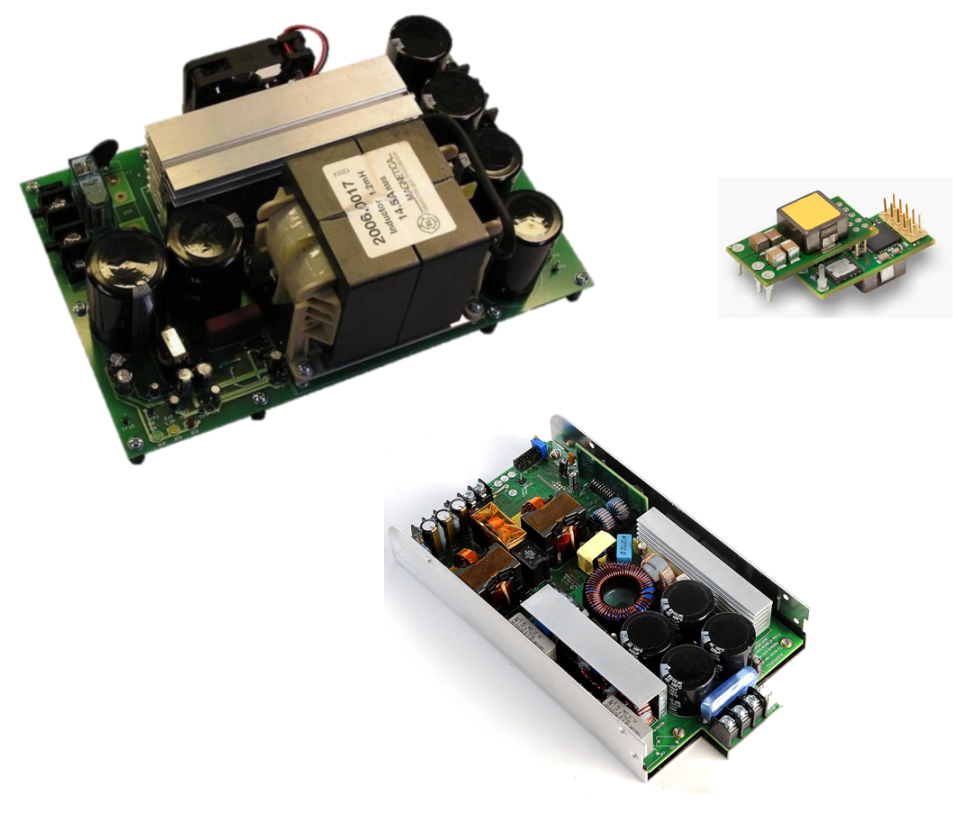
Figure 1: Modern Power Converter Size is Dominated by the Magnetic Components
Figure 1 shows modern power converters for different applications. A PFC circuit, LLC, and a point-of-load converter all feature prominent magnetics. In some cases, we find that the semiconductor devices no longer even need a heatsink and have disappeared from view underneath the circuit board. This emphasizes even more the need to work harder on the magnetics if we are to continue making progress with size reduction.
When starting a series of articles on magnetics design, it is customary to start at the beginning with design basics. Considerations of turns counts, saturation, core materials, and design optimization are usually at the forefront. You can learn more about some of these issues from ourmagnetics videos[1].
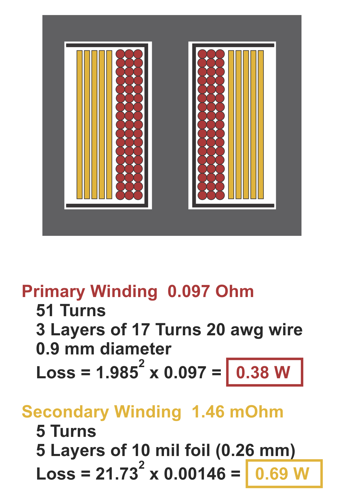
However, in this article, we are going to start with an advanced topic which causes severe problems for many designers. We will see in the example used in this article that conventional analysis of winding loss indicates that there will be just over 1 W of dissipation. However, detailed proximity loss analysis shows that, in reality, there isalmost 15 Wof power loss.
Forward Converter Design Example
Figure 2 shows an example forward converter running at 360 W. The converter runs at a switching frequency of 100 kHz. We will look at the detailed design of the transformer and show that it demonstrates excessive winding loss, despite initially good performance calculations.
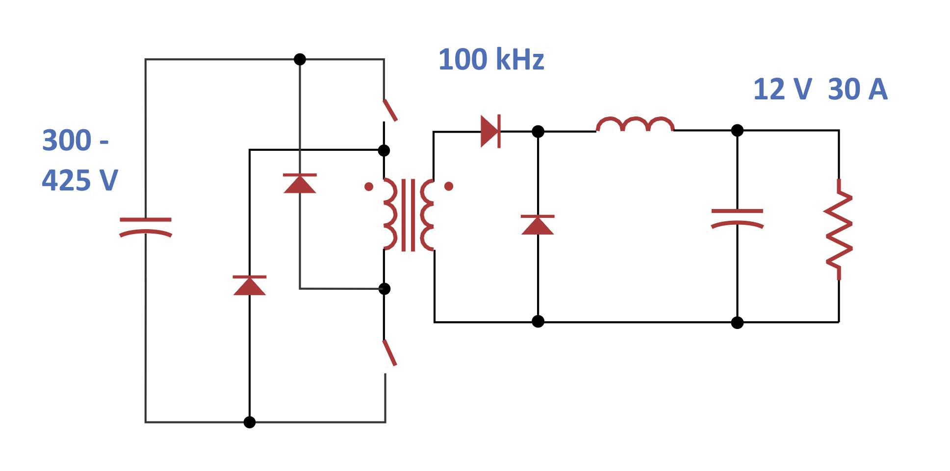
Figure 2: Two-Switch Forward Converter for 360 W Output


